| APPLICATION NOTE USM 101 |
Author: Mihaela Radulescu, M Phys. Sc. member technical staff, SEMICONIX CORPORATION |
|
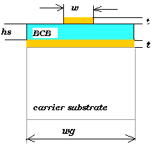
Thin-film microstrip lines (TFMSL) are miniaturized microstrip lines, (a
signal conductor, a dielectric and a ground conductor), located on top of
the silicon substrate or the carrier substrate. (Fig.1) The ground
metallization shields the line from the silicon substrate effects; therefore
low resistivity silicon substrates can be used without deteriorating
microwave performance. Using high-quality polymers as dielectric, e.g. BCB
or polyimide, TFMSLs have attenuation comparable with coplanar waveguides in
GaAs microwave integrated circuits. TFMSLs find more and more applications
in Si-based monolithic microwave integrated circuits and as transmission
lines in multichip modules.
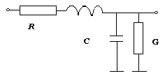
Fig.1 TFMSL cross section The propagation parameters of TFMSL can be precise and efficient described using a simplified model. The model used differs considerable from the conventional microstrip lines because of the differences in geometrical dimensions. For conventional microstrip lines height and width of the signal conductor are in the range of hundreds of microns. For TFMSLs these values are around 10 µm, in the order of magnitude of metallization thickness. Small dimensions increase conductor loss and finite metal conductivity and internal inductance have been taken into account. Phase constant and characteristic impedance deviate considerably from the lossless case and show typical increase toward lower frequencies known from coplanar waveguides.A distributed equivalent circuit model (Fig.2) can be used for describing TFMSLs.
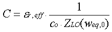
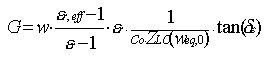
Fig.2 Distributed equivalent-circuit model of the TFMSL The elements of the equivalent circuit (the inductance per unit length L, the capacitance per unit length C, the resistance per unit length R and the conductance per unit length G) are related to different physical effects and can be determined separately. The model used to describe the dependence vs. frequency of the TFMSL parameters is practical and efficient and is based on the numerous approaches for microstrip lines available in the literature [1-5]. The capacitance per unit length can be calculated by means of Hammerstad and Jensen formulas[4] :
where co is free-space light velocity, er,eff is the effective relative dielectric constant, ZLO is the characteristic impedance for lossless case with t=0 and weq,0 is the equivalent signal conductor width without dielectric substrate, which takes into account the finite thickness of the signal conductor.The conductance per unit length G account for the dielectric loss of the substrate, described by the dielectric loss tangent, tan(de).
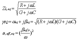
C and G/w are frequency independent up to the beginning of the non-TEM dispersion (well beyond 100 GHz for typical TFMSLs). The line resistance R and inductance L exhibit a considerable frequency dependence. The frequency dependence is determined by the change of current density distribution in the nonideal conductors, due to the varying current penetration into the conductors when increasing the frequency. At low frequencies near dc the current density is homogenous over all conductor cross sections. At high frequencies, the skin-effect range all the conductor dimensions are large compared with skin depth d and the current flows only in a shallow area at the conductor surface. Between these two regions there is a transient range that may be widely extended. Djorgjevic and Sarkar formulas [3] for R and L are used to calculate R and L for the entire frequency range, taking into account the external inductance covering the magnetic field outside of the conductor, the internal inductance describing the magnetic field inside the conductor, the conductor resistance under skin-effect and dc conditions. The propagation quantities, i.e. complex characteristic impedance ZL,eq, attenuation aeq and effective relative dielectric constant er,eff,eq can be determined based on the equivalent-circuit elements R,L,C,G. |
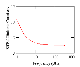
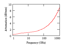
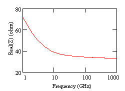
Fig.3,4,5 present effective relative dielectric constant, attenuation and real of characteristic impedance for a TFMSL with w=8µm, hs=1.7µm, t=0.8µm, wg=88µm, conductivity of the metallization k=2.5*107S/m, BCB with er=2.7 and tan(de)=0.015.
Fig.3. Effective relative dielectric constant vs.frequency
Fig.4. Attenuation vs.frequency
Fig.5. Real(Z) vs.frequency Accuracy of this model is established by comparing the line parameters to numerical full-wave simulation results, which takes into account conductor and dielectric losses [4].There are some geometrical limitations related to the metal thickness, signal and ground-conductor width, which restrict the range of validity of the model. But, once these conditions are fulfilled the model yields under 2% to 8% deviations for propagation quantities, an accuracy sufficient for application of the model in practical circuit design. The frequency range of validity extends down to dc and well into the submillimeter-wave range.
References |