|
Microstrip lines are widely used in the microwave integrated circuits from
hybrids to monolithics.The microstrip line is composed of a thin conducting
metal strip of width Wo, thickness t and length L placed on a nonmagnetic
dielectric substrate that is in turn placed on a conducting metal ground-plane.
The substrate has thickness T and relative permittivity er. The structure
is shown in figure 1. Above the conducting strip is a second dielectric
material, air.

Fig.1 Microstrip line structure
Zo,
the characteristic impedance, t, the propagation delay that depends on the
length of the line, and a, the attenuation constant, are the parameters used to
model the transmission line. All physical transmission media have some loss.
Considering a small segment of a lossy transmission line distributed circuit
model as show in figure 2, the losses in the transmission media are depicted by
the series and the shunt resistors. These resistors represent the finite
conductivity of the conductors and the dielectric insulator between the
conductors respectively. The constants R, G, L, and C are defined
as per unit length circuit parameters. The total length of the transmission line
segment is Dx.
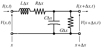
Fig.2 Distributed circuit model of a lossy transmission line.
The
advantages of using the microstrip line is that it is well suited for the
printed circuit fabrication process, and because the strip conductor is exposed
on the top side, component mounting is relatively easy. However, since the
dielectric around the conductor is inhomogeneous, EM fields can not propagate in
TEM mode. This is because a TEM wave must have a velocity c in the air
above the strip and one of

in
the substrate below. Because of the different velocities needed for TEM
propagation, it is not possible to form a single TEM mode. Consequently, small
amount of transverse fields must exist to equalize the propagation velocities in
different dielectrics. This hybrid presence of TE and TM modes form the
principle mode of propagation in a microstrip line which is named quasi-TEM
mode. At low frequencies, up to a few GHz, static analysis and TEM mode formulae
can be used to approximate the quasi-TEM transmission line characteristics. At
frequencies above that, dynamic analysis must be used to solve for all fields
components in order to characterize the microstrip line. For the microstrip line
in Fig. 1, the propagation velocity np and characteristic impedance Zc
can be approximated at low frequencies by applying the TEM mode equations 1 and
2 which are restated below.
If
we remove the dielectric substrate under the strip and fill it with air , the
transmission line is surrounded by homogeneous dielectric and true TEM mode can
propagate on the line.
where c is the speed of light in air. Since we assumed the dielectric
substrate in the microstrip line is nonmagnetic, i.e. µr=1, the per
unit length inductance L remains the same and one gets : The term C/Co
is called the effective relative permittivity of the microstrip line
er,eff
. Both C and CO can be found by solving the static field
equations for this structure. However, oncer,eff
is calculated from the static capacitances, the microstrip line can be
approximated by a TEM strip line surrounded homogeneously with dielectric whose
relative permittivity er,eff.
In dynamic analysis, although static capacitances are not defined
er,eff
is still being used by solving for phase velocity in the quasi-TEM mode ,
i.e. eq.7:
|
If
the width Wo of the microstrip line is changed smaller, both C and Co
decrease. Consequently, Zc becomes higher. Likewise, widening the line width
reduces its characteristic impedance. The effective relative permittivity also
changes with line width but not as obvious because of the ratio. In the case of
a very wide line almost all electric field lines are packed between the strip
and the ground plane with or without the substrate. Therefore, the ratio C/Co
is very close to the relative permittivity of the substrate er, but can
never quite become that. As the width of the line shrinks, proportionally more
and more field lines reach the air space above the substrate. As a result, the
ratio C/Co drops, but it can never reach 1. So, the effective relative
permittivity of the microstrip line increases as the width of the line
increases, decreases as the width of the line decreases. However, its value will
always be in between the relative permittivity of the substrate and the air,
i.e. 1<er,eff<er.
With the presence of transverse field components in the quasi-TEM transmission
lines, the characteristic impedance is not uniquely defined as of the TEM case.
This is because the voltage between the conductors depends on the integration
path chosen, and the longitudinal current flowing in the strip and the ground
plane are different. Although different definitions of characteristic impedance
for microstrip have been used in research articles, however, conventionally the
voltage is defined along the center line of the strip and the current is defined
as the longitudinal current in the strip itself. Approximate formulas for the
characteristic impedance have been derived by various methods in the articles
with about 1% accuracy which is more than sufficient in practice. The thickness
of the microstrip t is not to be taken into account for t/T<0.005.
Fig.3 and 4 present the evolution of the characteristic impedance and
er,eff
respectively vs. the ratio WO/T.
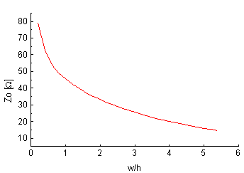
Fig.
3. Zo vs. Wo/T , dielectric Al2O3
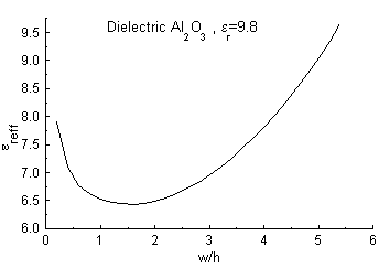
Fig.
4. ereff
vs. Wo/T, dielectric Al2O3
Sonnet Lite Software was used to analyze the behavior of the thin film
microstrip transmission lines vs. frequency with different length of stripeline
. Fig.5 presents S11 magnitudes for a microstrip transmission line with the
width of 9.5 mils, the length from 50 to 500 mils on Al2O3 dielectric 10 mils thick.
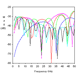
Fig.5 Mag(S11) vs.frequency for
Wo=9.5 mils, L=50,100,150,200,250 and 500 mils,
Al2O3 dielectric
er=9.8,
T=10 mils.
References
1. Joël
Redoutey "Calcul et applications des lignes microstrip"
2. E. Hammerstad and O. Jensen. "Accurate Models for Microstrip
Computer-Aided Design," MTT Symposium Digest, 1980, pp. 407-409.
3. A. C. Cangellaris, M. Celik, S. Pasha, and L. Zhao,"Electromagnetic
model order reduction for system-level modeling," IEEE Trans. Microwave Theory
Tech. , vol. 47, no. 6, pp. 840-849, 1999.
|