|
DC-DC CONVERTER CONTROL CIRCUITS
USM MC34063A
FEATURES
APPLICATIONS
DC-DC CONVERTER CONTROL CIRCUITS
Output switch current in excess of 1.5A
2% reference accuracy; Low quiescent current 2.5mA (TYP.)
Operating from 3V to 40V
Frequency operation 100KHz
Active current limiting
In DIE form, this device is an excellent selection for many chip and wire HYBRID CIRCUITS
PRODUCT DESCRIPTION AND SHORT APPLICATION NOTE
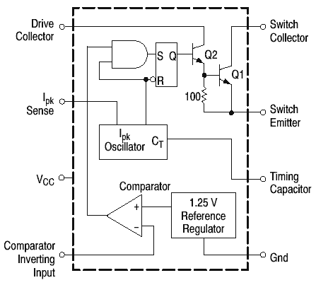
The USM MC34063A series is a monolithic control circuit delivering the main functions for DC-DC voltage converting. The device contains an internal temperature compensated reference, comparator, duty cycle controlled oscillator with an active current limit circuit, driver and high current output switch. Output voltage is adjustable through two external resistors with a 2% reference accuracy.
IC SCHEMATIC DIAGRAM
MAXIMUM RATINGS
PARAMETER SYMBOL VALUE UNITS
Power Supply Voltages VCC 40 Vdc
Comparator Input Voltage Range VIR -0.3 to +40 Vdc
Switch Collector Voltage VC(switch) 40 Vdc
Switch Emitter Voltage (VPin1= 40V) VE(switch) 40 Vdc
Switch Collector to Emitter Voltage VCE(switch) 40 Vdc
Driver Collector Voltage VC(driver) 40 Vdc
Driver Collector Current (Note 1.) IC(driver) 100 mA
Switch Current ISW 1.5 A
Operating Junction Temperature TJ 150 °C
Operating Ambient Temperature Range Ta 0 to +70 °C
Storage Temperature Range Tstg -65 to +150 °C
ONLY Proper die handling equipment and procedures should be employed. Stresses beyond listed absolute maximum ratings may cause permanent damage to the device.
ELECTRICAL CHARACTERISTIC
PARAMETER TEST CONDITIONS SYMBOL MIN TYP MAX UNITS
OSCILATOR
Frequency VPin5=0V, CT=1.0nF, TA=25°C fOSC 24 33 42 KHZ
Charge Current VCC=5.0V to 40V, TA=25°C Ichg 24 35 42 µA
Discharge Current VCC=5.0V to 40 V, TA=25°C Idischg 140 220 260 µA
Discharge to Charge Current Ratio Pin 7 to VCC, TA=25°C Idischg/Ichg 5.2 6.5 7.5
Current Limit Sense Voltage Ichg=Idischg, TA=25°C VIpk(sense) 250 300 360 mV
OUTPUT SWITCH (Note 1)
Saturation Voltage, Darlington Connection ISW=1.0A, Pins 1, 8 connected VCE(sat)
1.0 1.3 V
Saturation Voltage ISW=1.0A, RPin8=82 to VCC,
Forced ß20 VCE(sat) 0.45 0.7 V
DC Current Gain ISW=1.0A,VCE=5.0V,TA=25°C hFE 50 75
Collector Off-State Current VCE=40V IC(off) 0.01 100 µA
COMPARATOR
Threshold Voltage TA=25°C;
TA=Tlow to Thigh Vth 1.225
1.21 1.25
- 1.275
1.29 V
Threshold Voltage Line Regulation VCC=3.0 V to 40 V Regline 1.4 5.0 mV
Input Bias Current Vin=0V IIB -20 -400 nA
TOTAL DEVICE
Supply Current VCC=5.0 V to 40 V, CT=1.0 nF,
Pin 7=VCC, VPin5>Vth, Pin2=GND,
Remaining pins open ICC 4.0 mA
(NOTE 1)Low duty cycle pulse techniques are used during test to maintain junction temperature as close to ambient temperature as possible.
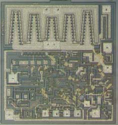
GENERAL DIE INFORMATION
Substrate Thickness (mils) Die size (mils) [mm] Bonding pads Backside metal
Silicon 10±1 (67.7x71.6) [1.72x1.82] min 4x4 mils, 1µm thick, aluminium Backside of the die is coated with 0.5µm GOLD , which makes it compatible with AuSi or AuGe die attach.
All US Microwaves products are available in die form. Typical delivery for die products is 2-3 weeks ARO. For Custom designs, delivery is 3-4 weeks ARO. Certain items may be available from stock. Inventory is periodically updated. All devices for chip and wire applications are 100% tested, visual inspected and shipped in waffle packs (WP). For high volume automated assembly, MIS chip capacitors are supplied as 4" wafers 100% tested, inked and diced on expanded film frame (FF).
TECHNOLOGY DESCRIPTION: SEMICONDUCTOR-MANUFACTURING
These integrated Circuits are manufactured with medium voltage junction isolated bipolar process. junction isolated bipolar processes allow integration of high performance NPN, PNP and JFET transistors, MOS capacitors, diffused resistors and precision thin film resistors. The bond pad metallization is standard 1µm Aluminium. The backside of the die is coated with 0.5µm GOLD , which makes it compatible with AuSi or AuGe die attach.
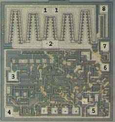
DIE LAYOUT - MECHANICAL SPECIFICATIONS
PAD # FUNCTION
1 Switch collector
2 Switch emitter
3 Timing capacitor
4 GND
5 Comparator Inverting Input
6 Vcc
7 Ipk sense
8 Driver Collector
STANDARD PRODUCTS ORDERING INFORMATION
STANDARD PRODUCTS PRICE LIST
USM PART # MINIMUM ORDER QUANTITY Waffle Packs U/P($)
USM MC34063A 100pc -WP $3.20
List prices are for standard products, available from stock.
List prices for other quantities and tolerances are available on line through Instant Quote.
For standard products available from stock, there is a minimum line item order. For custom products
please inquire by contacting US Microwaves technical sales. No rights can be derived from pricing
information provided on this website. Such information is indicative only, is showed for budgetary
use only and subject to change by US MICROWAVES at any time and without notice.
Products sold for space, military or medical applications, element evaluation and/or level K or S qualification are subject to minimum order levels to be established on a case by case basis. For any special applications, die level KGD qualification requirements, different packaging or custom configurations, contact sales department.
INSTANT QUOTE
US Microwaves P/N Quantity E-mail
ORDERING: Order on line at: http://www.usmicrowaves.com/porder.htm. A copy of the order along with an order confirmation receipt is issued instantly for all orders placed on line. On line Orders have to be verified, accepted and acknowledged by US Microwaves sales department in writing before, becoming non cancelable binding contracts.
DELIVERY: Typical delivery for die products packaged in waffle packs is 2-4 weeks ARO. For Custom designs, delivery is 3-5 weeks ARO. Certain items may be available from stock with delivery up to 1 week.
SHIPPING/PACKAGING: All devices for chip and wire applications are 100% tested, visual inspected and shipped in waffle packs (WP).
SAMPLES: Samples are available only for customers that have issued firm orders pending qualification of product in a particular application.
GUARANTEED SUPPLY! US Microwaves guarantees continuous supply and availability of all standard products provided minimum order quantities are met.
U.S. Microwaves has made every effort to have this information as accurate as possible. However, no responsibility is assumed by U.S. Microwaves for its use, nor for any infringements of rights of third parties which may result from its use. U.S. Microwaves reserves the right to revise the content or modify its product line without prior notice. U.S. Microwaves products are not authorized for and should not be used within support systems which are intended for surgical implants into the body, to support or sustain life, in aircraft, space equipment, submarine, or nuclear facility applications without the specific written consent of U.S. Microwaves.
|