|
Varactor diode, tuning diode: USMSMV30333-02 Single Varactor (Tuning) Diode 13pF same as kNOX SMV30333-07, kNOX SMV30333-07, kNOX SMV30333-07 kNOX SMV30333-07 manufactured by US Microwaves - Gold chip technology for known good varactor diode die, varactor diode flip chip, varactor diode bare die, wafer foundry for discrete semiconductors, microwave integrated circuits and advanced microwave components manufactured by US Microwaves
Varactor diode, tuning diode: USMSMV30333-02 Single Varactor (Tuning) Diode 13pF same as kNOX SMV30333-07, kNOX SMV30333-07, kNOX SMV30333-07 kNOX SMV30333-07 manufactured by US Microwaves - Gold chip technology for known good varactor diode die, varactor diode flip chip, varactor diode bare die, wafer foundry for discrete semiconductors, microwave integrated circuits and advanced microwave components manufactured by US Microwaves. Gold metallization for interconnections instead of aluminum or copper, for high reliability devices for system in package applications using silicon printed circuit boards, ceramic substrates or chip on board, assembled via flip chip or chip and wire.
Varactor diode, tuning diode: USMSMV30333-02 Single Varactor (Tuning) Diode 13pF same as kNOX SMV30333-07,
kNOX SMV30333-07, kNOX SMV30333-07 kNOX SMV30333-07 manufactured by US Microwaves - Gold chip technology for known good
varactor diode die, varactor diode flip chip, varactor diode bare die, wafer foundry for discrete semiconductors,
microwave integrated circuits and advanced microwave components manufactured by US Microwaves Varactor diode, tuning
diode: USMSMV30333-02 Single Varactor (Tuning) Diode 13pF same as kNOX SMV30333-07, kNOX SMV30333-07, kNOX SMV30333-07
kNOX SMV30333-07 manufactured by US Microwaves - Gold chip technology for known good varactor diode die, varactor diode
flip chip, varactor diode bare die, wafer foundry for discrete semiconductors, microwave integrated circuits and
advanced microwave components manufactured by US Microwaves. Gold metallization for interconnections instead of
aluminum or copper, for high reliability devices for system in package applications using silicon printed circuit
boards, ceramic substrates or chip on board, assembled via flip chip or chip and wire. US MICROWAVES Single Varactor
(Tuning) Diode 13pF Advanced Microwave Components USMSMV30333-02 - FLIP CHIP FEATURES APPLICATIONS VARACTOR DIODE -
FLIP CHIP Gold metallization RoHS compliant, Lead Free High reliability flip chip Unique new design Compatible with
both chip and wire, flip chip and surface mount assembly. Chip on Board, System in package SIP Hybrid Circuits
Parametric amplifiers, Parametric Oscillators Voltage-controlled oscillators, PLL circuits Frequency synthesizers
USMSMV30333-02 SMV30333-07 Single Varactor (Tuning) Diode 13pF VARACTOR DIODES - PRODUCT DESCRIPTION AND SHORT
APPLICATION NOTE Varicap Diode, Varactor Diode, Variable Capacitance Diode or Tuning Diode is a type of diode which has
a variable capacitance that is a function of the voltage impressed on its terminals. Varactors are operated
reverse-biased so no current flows, but since the thickness of the depletion zone varies with the applied bias voltage,
the capacitance of the diode can be made to vary. Generally, the depletion region thickness is proportional to the
square root of the applied voltage; and capacitance is inversely proportional to the depletion region thickness. Thus,
the capacitance is inversely proportional to the square root of applied voltage. All diodes exhibit this phenomenon to
some degree, but specially made varactor diodes exploit the effect to boost the capacitance and variability range
achieved - most diode fabrication attempts to achieve the opposite. Varactors are principally used as a
voltage-controlled capacitor, rather than as rectifiers. They are commonly used in parametric amplifiers, parametric
oscillators and voltage-controlled oscillators as part of phase-locked loops and frequency synthesizers. Flip Chip
Varactor diode series are available in die form in four different pad compositions: -FC, -GB, -GT and -AN. These
products are ideal for high reliability hybrid circuits, multi chip module applications and surface mount applications.
HIGH RELIABILITY BARE DIE AND SYSTEM IN PACKAGE - SHORT APPLICATION NOTE COB (Chip on Board) and SiP
(System-in-Package) are integrating proven mature products in bare die of mixed technologies i.e. Si, GaAs, GaN, InP,
passive components, etc that cannot be easily implemented in SOC (System-on-Chip) technology. COB and SiP have small
size footprint, high density, shorter design cycle time, easier to redesign and rework, use simpler and less expensive
assembly process. For extreme applications the bare die has to withstand also harsh environmental conditions without
the protection of a package. KGD, Known Good Die concept is no longer satisfactory if the die cannot withstand harsh
environmental conditions and degrades. Standard semiconductor devices supplied by many manufacturers in bare die are
build with exposed aluminum pads that are extremely sensitive to moisture and corrosive components of the atmosphere.
US Microwaves has reengineered industry standard products and now offers known good die for bare die applications with
gold interconnection and well-engineered materials that further enhance the die reliability. US Microwaves also offers
Silicon Printed Circuit Board technology with integrated passive components as a complete high reliability SIP solution
for medical, military and space applications. DISCRETE SEMICONDUCTORS MANUFACTURING PROCESS Discrete semiconductors are
manufactured using US Microwaves in house high reliability semiconductor manufacturing processes. All semiconductor
devices employ precision doping via ion implantation, silicon nitride junction passivation, platinum silicided contacts
and gold interconnect metallization for best performance and reliability. MNOS capacitors, Tantalum Nitride TaN or
Sichrome SiCr thin film resistors are easily integrated with discrete semiconductors on same chip to obtain standard
and custom complex discrete device solutions. All thin film microwave products are manufactured using advanced
semiconductors and thin film technologies including ultra-stable and self passivating Tantalum Nitride resistors, gold
interconnect metallization and reliable MNOS capacitors to achieve excellent uniformity, performance and reliability.
Thin film technology is the preferred solution for all applications that require low noise, long term stability and
excellent performance at very high frequencies. US Microwaves employs proprietary thin film technologies for deposition
of a wide range of resistive films with sheet resistance films from 1Ω/sq to 10,000Ω/sq. All US Microwaves products
are available in die form and are ideal for high reliability hybrid and multi chip module applications. All US
Microwaves products are manufactured using GOLD CHIP TECHNOLOGY™ a trade mark of Semiconix Corporation. Maximum
Ratings at TA = 25°C, unless otherwise specified Parameter Symbol Value Unit Operating temperature range Top -55 to +
125° C °C Storage temperature Tstg -65 to + 150° C °C Electrical Characteristics at TA= 25°C, unless otherwise
specified Name Symbol Test Conditions Value Unit Min. Typ. Max Reverse Breakdown Voltage V(BR)R IR=10 µA 8 V Reverse
current IR1 VR=6 V 100 nA Diode capacitance CT1 VR=1.65 V f=1MHz 11 14 pF Capacitance ratio C0.3/C1.65 VR=0.3 V,
VR=1.65 V,f=1MHz 3 4 Capacitance ratio C1.65/C3 VR=1.65 V, VR=3 V,f=1MHz 3 4 Capacitance ratio CT1/CT10 Capacitance
ratio CT2/CT20 Series resistance rS f=50MHzVR=4V 9 Ω CROSS REFERENCE PARTS: kNOX SMV30333-07, kNOX SMV30333-07, kNOX
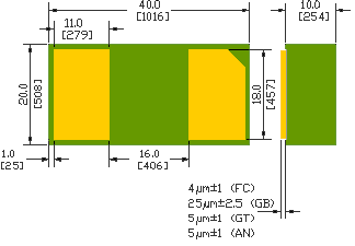
SMV30333-07 GENERAL DIE INFORMATION Substrate Thickness [mils] Size mm [mils] Bonding pads dimensions per drawing
Backside Silicon 10±2 0402 1.02x0.51 [40x20] Type Pad metal Thickness Assembly -FC TiW/Au 4µm±1 Wire bonding or
Silver epoxy -GB TiW/Au 25µm±2.5 Thermosonic -GT Ti/Pt/AuSn 5µm±1 Reflow -AN Ni/Au 5µm±1 Solder reflow Optional
backside coating and/or marking. LAYOUT / DIMENSIONS / PAD LOCATIONS Click to select process: -FC -GB -GT -AN
USMSMV30333-02 kNOX SMV30333-07, kNOX SMV30333-07, kNOX SMV30333-07 kNOX SMV30333-07 Single Varactor (Tuning) Diode
13pF USMSMV30333-02 kNOX SMV30333-07, kNOX SMV30333-07, kNOX SMV30333-07 kNOX SMV30333-07 Single Varactor (Tuning)
Diode 13pF wire bonding USMSMV30333-02 kNOX SMV30333-07, kNOX SMV30333-07, kNOX SMV30333-07 kNOX SMV30333-07 Single
Varactor (Tuning) Diode 13pFthermosonic USMSMV30333-02 kNOX SMV30333-07, kNOX SMV30333-07, kNOX SMV30333-07 kNOX
SMV30333-07 Single Varactor (Tuning) Diode 13pFthermal USMSMV30333-02 kNOX SMV30333-07, kNOX SMV30333-07, kNOX
SMV30333-07 kNOX SMV30333-07 Single Varactor (Tuning) Diode 13pFsolder reflow USMSMV30333-02 kNOX SMV30333-07, kNOX
SMV30333-07, kNOX SMV30333-07 kNOX SMV30333-07 Single Varactor (Tuning) Diode 13pF SEMICONDUCTOR ASSEMBLY PROCESS -
SHORT APPLICATION NOTE US Microwaves flip chip components are designed for dry assembly processes as well as for
processes that use adhesives, fluxes etc. Dry assembly process is an assembly process that does not use additional
solders, fluxes or adhesives. Thermosonic wire bonding is a dry assembly process. US Microwaves Flip Chip -FC series
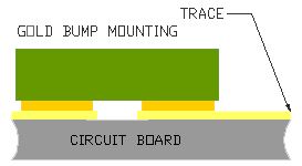
can be also used for thermosonic wire bonding. US Microwaves Gold Bump -GB series are flip chips that are
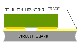
thermosonically attached to a circuit. US Microwaves Gold Tin -GT series are flip chips with Au/Sn, 80/20 metallized
pads. GT series can be attached to circuits by bringing the die in contact with a substrate which temperature is more
than 280°C. Upon cooling bellow 280C, the die is firmly welded to the substrate. Flux less dry assembly is most
reliable but is also most expensive because of thick gold bumps or expensive Au/Sn process. US Microwaves -FC series is
designed to be used for flip chip assembly with conductive silver epoxy. It is a simple and inexpensive process
consisting of 3 steps: - transfer a thin conductive epoxy layer onto the bonding pads; -align to substrate and attach;
-cure silver epoxy and inspect. Same procedure may be used also with -GB series in certain applications. US Microwaves
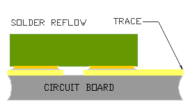
Gold/Nickel -AN series is the most efficient wafer level chip size package W-CSP designed for mixed surface mount and
flip chip applications. The assembly process is same as for packaged surface mount components. The process consist of
at least 3 steps; -screen print solder paste on the printed circuit board; -flip chip, align and attach to the tacky
solder paste; -dry paste, reflow at T>220°C, clean, etc. US Microwaves Flip Chip -AN series are available in many
sizes with landing pads compatible with the industry standard CSP as well as surface mount packages. STANDARD PRODUCTS
ORDERING INFORMATION VERSION SMX P/N WAFFLE PACKS QUANTITY U/P($) FILM FRAME MIN QUANTITY U/P($) Flip chip
USMSMV30333-02-FC -WP 10000 -FF 45000 Flip chip USMSMV30333-02-FC -WP 50000 -FF 225000 Gold Bump USMSMV30333-02-GB -WP
10000 -FF 45000 Gold Bump USMSMV30333-02-GB -WP 50000 -FF 225000 Gold-Tin USMSMV30333-02-GT -WP 10000 -FF 45000
Gold-Tin USMSMV30333-02-GT -WP 50000 -FF 225000 Gold/Nickel USMSMV30333-02-AN -WP 10000 -FF 45000 Gold/Nickel
USMSMV30333-02-AN -WP 50000 -FF 225000 LEAD TIMES - Typical delivery for standard products is 4-6 weeks ARO. For custom
devices consult factory for an update on minim orders and lead times. CONTINOUS SUPPLY - US Microwaves guarantees
continuous supply and availability of any of its standard products provided minimum order quantities are met. CUSTOM
PRODUCTS - For custom products sold as tested, bare die or known good die KGD, there will be a minimum order quantity
MOQ. Dice are 100% functional tested, visual inspected and shipped in antistatic waffle packs. For high volume and pick
and place applications, dice are also shipped on film frame -FF. For special die level KGD requirements, different
packaging or custom configurations, contact sales via CONTACTS page. SAMPLES - Samples are available only for customers
that have issued firm orders pending qualification of product in a particular application. ORDERING - US Microwaves
accepts only orders placed on line by registered customers. On line orders are verified, accepted and acknowledged by
US Microwaves sales department in writing. Accepted orders are non cancelable binding contracts. SHIPING - Dice are
100% functional tested, visual inspected and shipped in antistatic waffle packs. For high volume and pick and place
applications, dice are also shipped on film frame -FF. Products sold for space, military or medical applications,
element evaluation and/or level K or S qualification are subject to minimum order levels to be established on a case by
case basis. For any special applications, die level KGD qualification requirements, different packaging or custom
configurations, contact sales department. /cgi-bin/rfq.cgi" method="post" target="new">
INSTANT QUOTE US Microwaves P/N Quantity E-mail ORDERING: Order on line HERE. A copy of the order along with an order
confirmation receipt is issued instantly for all orders placed on line. On line Orders have to be verified, accepted
and acknowledged by US Microwaves sales department in writing before, becoming non cancelable binding contracts.
DELIVERY: Typical delivery for die products packaged in waffle packs is 2-4 weeks ARO. For Custom designs, delivery is
3-5 weeks ARO. Certain items may be available from stock with delivery up to 1 week. SHIPPING/PACKAGING: All devices
for chip and wire applications are 100% tested, visual inspected and shipped in waffle packs (WP). For larger
orders,>10k pc, devices can be shipped on film frame. For smaller quantities, it may vary. For high volume automated
assembly, devices may be supplied as 4" wafers 100% tested, inked and diced on expanded film frame (FF). SAMPLES:
Samples are available only for customers that have issued firm orders pending qualification of product in a particular
application. GUARANTEED SUPPLY! US Microwaves guarantees continuous supply and availability of all standard products
provided minimum order quantities are met. U.S. Microwaves has made every effort to have this information as accurate
as possible. However, no responsibility is assumed by U.S. Microwaves for its use, nor for any infringements of rights
of third parties which may result from its use. U.S. Microwaves reserves the right to revise the content or modify its
product line without prior notice. U.S. Microwaves products are not authorized for and should not be used within
support systems which are intended for surgical implants into the body, to support or sustain life, in aircraft, space
equipment, submarine, or nuclear facility applications without the specific written consent of U.S. Microwaves. Home
Product Tree Tech. Support PDF Request Quote Inventory Place Order Contact sales Last updated: US MICROWAVES www.semiconix-semiconductor.com Tel:(408)986-8026 Fax:(408)986-8027 ©1990- US MICROWAVES All rights reserved. No
material from this site may be used or reproduced without permission.
|


