|
VERY LOW DROPOUT VOLTAGE REGULATORS USM L4805
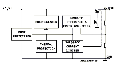
The USM L4805 series devices are voltage regulator with a very low voltage drop ( typically 0.4 V at fullrated current), output current up to 400mA, low current and comprehensive on-chip protection. The-quiescentse devices are protected against load dump and field decay transients of ±60V, polarity reversal and overheating. A foldback current limiter protects against load short circuits. Available in 5V, 8.5V 9.2V, 10V and 12V versions ( all ±4%, TI = 25°C ) the-quiescentse regulators are designed for automotive, industrial and consumer applications where low consumption is particularly important.
Input/Output Typ. 0.4V 400mA Output Current Low Quiescent Current Reverse Polarity Protection Over Voltage Protection (±60V) Foldback Current Limiting
Thermall Shutdown In DIE form, this device is an excellent selection for many chip and wire HYBRID CIRCUITS
DC Input Voltage +35 V DC Input Reverse Voltage -18 V Transient Input Overvoltages LoadDump: 5ms =< Trise =<10ms,
tf Fall Time Constant = 100ms, Rsource =< 0.5 FieldDecay: 5ms =< Tfall =< 10ms,Rsource =< 10
tr Rise Time Constant = 33ms Junction and Storage Temperature Range -55 to +150 °C ONLY Proper die handling equipment and procedures should be employed.
Stresses beyond listed absolute maximum ratings may cause permanent damage to the device.
ELECTRICAL CHARACTERISTIC VI=14.4V;CO=100F;Tj=25°C unless otherwise specified. PARAMETER SYMBOL TEST CONDITIONS MIN TYP LIMIT UNITS
Output Voltage VO IO=5mA to 400mA 4.8 5.0 5.2 V Operating Input Voltage VI 26 V Line Regulation DVO/VO VI=13 to 26V; IO=5mA 1 10 mV/V
Load Regulation DVO/VO IO= 5 to 400mA* 3 15 mV/V Dropout Voltage VI-VO IL = 150mA
IL = 400mA* 0.2 0.4 0.4 0.7 V QuiescentCurrent Iq IL = 0mA IL = 150mA IL = 400mA * 0.8 25 65 2 45 90 mA
Temperature Output Voltage Drift DVO/DT*VO 0.1 mV/°C*V
Supply Voltage Rejection SVR IO=350mA;f=320Hz; CO=100F;VI=VO+3V+2Vpp 60 dB Maximum Output Current IO 800 mA
Output Short Circuit Current (fold back condition) ISC 350 500 mA ELECTRICAL CHARACTERISTIC VI=14.4V;CO=100F;Tj=-40to125°C (note1) unless otherwise specified.
PARAMETER SYMBOL TEST CONDITIONS MIN TYP LIMIT UNITS Output Voltage VO IO=5mA to 400mA 4.70 5.0 5.30 V
Operating Input Voltage VI Note 2 26 V Line Regulation DVO/VO VI=13 to 26V; IO=5mA 2 15 mV/V
Load Regulation DVO/VO IO=5 to 400mA* 5 25 mV/V Dropout Voltage VI-VO IL = 150mA IL = 400mA* 0.25
QuiescentCurrent Iq IL = 0mA IL = 150mA IL = 400mA * Mximum Output Current IO 870 mA Output Short Circuit Current (fold back condition) ISC 230 mA
(NOTE 1) This limits are guaranteed by design, correlation and statistical control on production samples ove rthe indicated temperature and supply voltage ranges.
(NOTE 2) For a DC voltage 26V < 35V the device is not operating.
|