The USM LP2951-5.0 series are micropower voltage regulators with very low quiescent current (75µA typ.) and very low drop out voltage (typ.40 mV at light loads and 380 mV at 100mA). They are ideally suited for use in battery-powered systems. Furthermore, the quiescent current of the LP2951 increases only slightly in drop out, prolonging battery life. The 8-lead LP2951 is available in die form. One such feature is an error flag output which warns of a low output voltage, often due to falling batteries on the input. It may be used for a power-on reset. A second feature is the logic-compatible shut down in put which enables the regulator to be switched on and off. Also, the part may be pin-strapped for a 5V,3V,or 3.3V output (depending on the version), or programmed from 1.24V to 29V with an external pair of resistors. Careful design of the LP2951 has minimized all contributions to the error budget. This includes a tight initial tolerance (0.5% typ.), extremely good load and line regulation (0.05% typ.)and a very low output voltage temperature coefficient, making the part useful as a low-power voltage reference.


US MICROWAVES
Advanced Microwave Components
  100mA Low Dropout Voltage Regulators
USM LP2951-5.0


FEATURES
APPLICATIONS
LDO VOLTAGE REGULATOR
High accuracy output voltage
Guaranted 100mA output
Very low quiescent current
Low dropout voltage
Extremely tight load and line regulation
Very low temperature coefficient
Needs only 1µF for stability; Error Flag warms of output dropout
Logic-Controlled electronic shutdown
Output programmable from 1.24 to 29V.
In DIE form, this device is an excellent selection for many chip and wire HYBRID CIRCUITS

PRODUCT DESCRIPTION AND SHORT APPLICATION NOTE
The USM LP2951-5.0 series are micropower voltage regulators with very low quiescent current (75µA typ.) and very low drop out voltage (typ.40 mV at light loads and 380 mV at 100mA). They are ideally suited for use in battery-powered systems. Furthermore, the quiescent current of the LP2951 increases only slightly in drop out, prolonging battery life. The 8-lead LP2951 is available in die form. One such feature is an error flag output which warns of a low output voltage, often due to falling batteries on the input. It may be used for a power-on reset. A second feature is the logic-compatible shut down in put which enables the regulator to be switched on and off. Also, the part may be pin-strapped for a 5V,3V,or 3.3V output (depending on the version), or programmed from 1.24V to 29V with an external pair of resistors. Careful design of the LP2951 has minimized all contributions to the error budget. This includes a tight initial tolerance (0.5% typ.), extremely good load and line regulation (0.05% typ.)and a very low output voltage temperature coefficient, making the part useful as a low-power voltage reference.


IC SCHEMATIC DIAGRAM

MAXIMUM RATINGS
PARAMETER SYMBOL VALUE UNITS
Power disipation   Internal limited  
Storage temperature Range   -65 to +150 °C
Operating Junction Temperature Range TJ -55 to +150 °C
Output Voltage VOUT 5.0 V
Input Supply Voltage   -0.3 to +30 V
Feedback Input Voltage   -1.5 to +30 V
Shutdown Input Voltage   -0.3 to+30V V
Error Comparator Output   -0.3 to +30 V
ONLY Proper die handling equipment and procedures should be employed. Stresses beyond listed absolute maximum ratings may cause permanent damage to the device.

ELECTRICAL CHARACTERISTIC
(Ta=25°C, VIN=15V, unless otherwise specified)
PARAMETER TEST CONDITIONS MIN TYP MAX UNITS
Output Voltage 25°C<Tj<85°C
Full Operating Temperature
0.985 |Vo|
0.98 |Vo|
Vo 1.015 |Vo|
1.02 |Vo|
V
Output Voltage 100µA<IL<100mA,
TJ<TJMAX
0.976 |Vo Vo 1.024 |Vo| V
Output Voltage Note1   50 150 ppm/°C
Line Regulation(Note3) VO+1V<Vm<30V(Note4)   0.04 5.075 %
Load Regulation (Note3) 100µA<IL<100mA   0.1 0.3 %
Dropout Voltage (Note 3) IL=100µA
IL=100mA
  50
380
80
450
mV
Ground Current IL=100µA
IL=100mA
  75
8
120
12
µA
mA
Dropout Ground Current Vin=V0-0.5V
IL=100µA
  110 170 µA
Current Limit Vout=0   160 200 mA
Thermal Regulation     0.05 0.2 %/W
Output Noise, 10Hz to 100 kHz CL=1µF
CL=200µF
CL=3.3µF
(Bypass=0.01µF pins 7 to 1)
  430
160
100
  µVrms
Reference Voltage   1.21 1.235 1.26 V
Reference Voltage Over Temperature (Note6) 1.185   1.285 V
Feedback pin Bias Current     20 40 µA
Reference Voltage Temperature Coefficient     5   ppm/°C
Feedback Pin Bias Current Temperature Coefficient     0.1   µA/°C
ERROR COMPARATOR
Output Leakage Current VV   0.01 1.0 µA
Output Low Voltage Vin=4.5V,IOL=400µA   150 250 mV
Upper Threshold Voltage (Note 8) 40 60   mV
Lower Threshold Voltage (Note 8)   75 95 mV
Hysteresis (Note 8)   15   mV
SHUTDOWN INPUT
Input logic Voltage Low (Regulator ON)
High (Regulator OFF)
2 1.3 0.7 V
Shut down Pin Input Current VS=2.4V
VS=30V
  30
450
50
600
µA
Regulator Output Current in Shutdown (Note9)
Vout=5.0V
  3 10 µA
 
(NOTE 1) Output or reference voltage temperature coefficients defined as the worst case voltage change divided by the total temperature range.
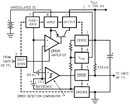
(NOTE 2) Unless otherwise specified all limits guaranteed for TJ=25°C, Vin=V0+1V, IL=100µA and CL=1µF. Additional conditions for the 8-pin versions are feedback tied to - XX V tap and output tied to output Sense (Vout=XX V) and Vshutdown<0.8V
(NOTE 3) Regulations is measured at constant junction temperature,using pulse testing with a low duty cycle. Changes in output voltage due to heating effects are covered under the specification for thermal regulation.
(NOTE 4) Line regulation for LP2951 -XX is tested at 150°C for IL=1mA. For IL=100µA and TJ=125°C, line regulation is guranteed by design 0.2%. See typical performance characteristics for temperature and load current.
(NOTE 5) Dropout voltage is defined as the input to differential at which the output voltage drops 100mV below its nominal value measured at 1V differential. At very low values of programmed output voltage, the minimum input supply voltage off 2V (2.3V over temperature )must be taken into account.
(NOTE 6) Vref<Vout<Vin-1V, 2.3V<Vin<30V, 100µA<IL<100mA,TJ<TJMAX
(NOTE 7) Output or reference voltage temperature coeffecient is defined as the worst case voltage change divided by the total temperature range
(NOTE 8) Comparator thresholds are expressed in terms of voltage differential at the feedback terminal below the nominal reference voltage measured at V0+1V input. To express these thresholds in therms of output voltage change, multiply by the error amplifier gain = Vout/Vref=(R1 +R2)/R2. For example at a programmed output is guaranteed to go low when the output drops by 95mVx5V/1.235V = 384mV. Thresholds remain constant as a percent of Vout as Vout is varied, with the dropout warning occuring at typically 5% below nominal, 7,5% guaranteed.
(NOTE 9) Vshutdown>2V, Vin<30V, Vout=0, Feedback pin tied to - XX V Tap

GENERAL DIE INFORMATION
Substrate Thickness (mils) Die size (mils) [mm] Bonding pads Backside metal
Silicon 10±1 (80.7x45.276) [2.05x1.15] min 4x4 mils, 1µm thick, aluminium Backside of the die is coated with 0.5µm GOLD , which makes it compatible with AuSi or AuGe die attach.
All US Microwaves products are available in die form. Typical delivery for die products is 2-3 weeks ARO. For Custom designs, delivery is 3-4 weeks ARO. Certain items may be available from stock. Inventory is periodically updated. All devices for chip and wire applications are 100% tested, visual inspected and shipped in waffle packs (WP). For high volume automated assembly, MIS chip capacitors are supplied as 4" wafers 100% tested, inked and diced on expanded film frame (FF).

TECHNOLOGY DESCRIPTION: SEMICONDUCTOR-MANUFACTURING
These integrated Circuits are manufactured with medium voltage junction isolated bipolar process. junction isolated bipolar processes allow integration of high performance NPN, PNP and JFET transistors, MOS capacitors, diffused resistors and precision thin film resistors. The bond pad metallization is standard 1µm Aluminium. The backside of the die is coated with 0.5µm GOLD , which makes it compatible with AuSi or AuGe die attach.
All US Microwaves products are manufactured using GOLDCHIP TECHNOLOGY™ a trade mark of Semiconix Corporation.

DIE LAYOUT - MECHANICAL SPECIFICATIONS
PAD # FUNCTION X(mils) X(mm) Y(mils) Y(mm)
1 OUTPUT 17.323 0.440 4.331 0.110
2 SENSE 31.890 0.810 4.331 0.110
3 SHUTDOWN 49.213 1.250 4.331 0.110
4 GROUND 73.425 1.865 4.331 0.110
5 ERROR 73.425 1.865 37.402 0.950
6 XX V TAP 36.811 0.935 37.402 0.950
7 FEEDBACK 28.937 0.735 37.402 0.950
8 INPUT 17.323 0.440 37.402 0.950
 

STANDARD PRODUCTS ORDERING INFORMATION

STANDARD PRODUCTS PRICE LIST
USM PART # MINIMUM ORDER QUANTITY Waffle Packs U/P($)
USM LP2951-5.0 100pc -WP $3.20
List prices are for standard products, available from stock. List prices for other quantities and tolerances are available on line through Instant Quote. For standard products available from stock, there is a minimum line item order. For custom products please inquire by contacting US Microwaves technical sales. No rights can be derived from pricing information provided on this website. Such information is indicative only, is showed for budgetary use only and subject to change by US MICROWAVES at any time and without notice.
Products sold for space, military or medical applications, element evaluation and/or level K or S qualification are subject to minimum order levels to be established on a case by case basis. For any special applications, die level KGD qualification requirements, different packaging or custom configurations, contact sales department.

INSTANT QUOTE
US Microwaves P/N Quantity E-mail    
 

ORDERING: Order on line at: http://www.usmicrowaves.com/porder.htm. A copy of the order along with an order confirmation receipt is issued instantly for all orders placed on line. On line Orders have to be verified, accepted and acknowledged by US Microwaves sales department in writing before, becoming non cancelable binding contracts.
DELIVERY: Typical delivery for die products packaged in waffle packs is 2-4 weeks ARO. For Custom designs, delivery is 3-5 weeks ARO. Certain items may be available from stock with delivery up to 1 week.
SHIPPING/PACKAGING: All devices for chip and wire applications are 100% tested, visual inspected and shipped in waffle packs (WP).
SAMPLES: Samples are available only for customers that have issued firm orders pending qualification of product in a particular application.

GUARANTEED SUPPLY! US Microwaves guarantees continuous supply and availability of all standard products provided minimum order quantities are met.

U.S. Microwaves has made every effort to have this information as accurate as possible. However, no responsibility is assumed by U.S. Microwaves for its use, nor for any infringements of rights of third parties which may result from its use. U.S. Microwaves reserves the right to revise the content or modify its product line without prior notice. U.S. Microwaves products are not authorized for and should not be used within support systems which are intended for surgical implants into the body, to support or sustain life, in aircraft, space equipment, submarine, or nuclear facility applications without the specific written consent of U.S. Microwaves.

Home Product Tree Tech. Support Print PDF Request Quote Inventory Place Order Contact sales

Last updated: July 01, 2009
US MICROWAVES | Tel:408-758-8690 Fax: 408-986-8027 | USMICROWAVES

©1990-2024 US MICROWAVES All rights reserved. No material from this site may be used or reproduced without permission.