|
TIMER
USM LM 555
FEATURES
APPLICATIONS
VOLTAGE REGULATOR
Direct replacement for SE555/NE555
Timing from micro-seconds through hours
Operates in both astable and mono- stable modes
Adjustable duty cycle
Output can source or sink 200mA
Output and supply TTL compatible
Temperature stability better than 0.005% per C
Normally on and normally off output
In DIE form, this device is an excellent selection for many chip and wire HYBRID CIRCUITS
PRODUCT DESCRIPTION AND SHORT APPLICATION NOTE
The USM LM555 is a highly stable device for generating accurate time delays or oscillation. Additional terminals are provided for triggering or resettin desired. In the time delay mode of operation, the time is precisely controlled by one external resistor and capacitor. For a stable operation as an oscillator, the free running frequency and duty cycle are accurately controlled with two external resistors and one capacitor.The circuit may retriggered and reset on falling waveforms, and the output circuit can source or sink up to 200mA or drive TTL circuits.
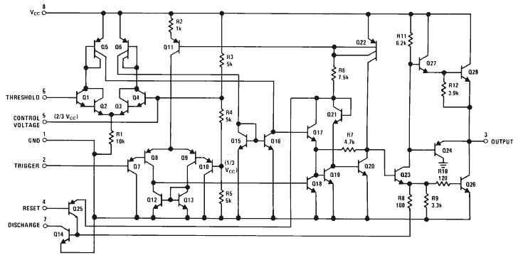
IC SCHEMATIC DIAGRAM
MAXIMUM RATINGS
PARAMETER VALUE UNITS
Supply Voltages +18 V
Power Disipation(Note3) LM555CM, LM555CN
LM555CMM 1180
603 mW
Operating Temperature Ranges LM555C 0 to +70 °C
Storage Temperature Range -65 to +150 °C
ONLY Proper die handling equipment and procedures should be employed. Stresses beyond listed absolute maximum ratings may cause permanent damage to the device.
ELECTRICAL CHARACTERISTIC
(Note 1,2 TA=25°C,VCC=+5V to+15V unless otherwise specificed)
PARAMETER TEST CONDITIONS MIN TYP MAX UNITS
Supply Voltage 4.5 16 V
Supply Curent VCC=5V R=¥
VCC=5V RL=¥
(Low State)Note4 3
10 6
15 mA
Timing Error, Monostable
Initial Accuracy
Drift with Temperature
Accuracy overTemperature
Drift with Supply
RA=1k to 100kW
C=0.1µF(Note 5)
1
50
1.5
0.1
%
ppm/C
%
%/V
Timing Error,Astable
Initial Accuracy
Drift with Temperature
Accuracy overTemperature
Drift with Supply RA,RB=1k to 100kW
C=0.1µF(Note 5) 2.25
150
3.0
0.30
%
ppm/C
%
%/V
Treshold Voltage 0.667 x VCC
Trigger Voltage VCC=15V
VCC=5V 5
1.67 V
Trigger Current 0.4 0.5 1 µA
Reset Voltage 0.4 0.5 1 V
Reset Current 0.1 0.4 mA
Threshold Current Note6 0.1 0.25 µA
Control Voltage Level VCC=15V
VCC=5V 9
2.6 10
3.33 11
4 V
Pin Discharge Leakage Output High 1 100 nA
Pin Discharge Sat
Output Low
Output Low VCC=15V,IZ=15mA
VCC=4.5V,IZ=4.5mA 180
80 200 mV
Output Voltage Drop (Low) VCC=15V
ISINK=10mA
ISINK=50mA
ISINK=100mA
ISINK=200mA
VCC=5V
ISINK=8mA
ISINK=5mA
0.1
0.4
2
2.5
0.25
0.25
0.75
2.5
0.35
V
Output Voltage Drop (High) ISOURCE=200mA VCC=15V
ISINK=100mA ,VCC=15V
VCC=5V 12.75
2.75 12.5
13.3
3.3 V
Rise Time of Output 100 ns
Fall Time of Output 100 ns
(NOTE 1)All voltages are measured with respect to the ground pin, unless otherwise specified.
(NOTE 2)Absolute Maximum Ratings indicate limits be yond which damage to the device may occur.Operating Ratings indicate conditions for which thedevice is functional,but do not guarantee specific performance limits.Electrical Characteristics state DC and AC electrical specifications under particular test conditions which guarantee specific performance limits.This assumes that the deviceis within the Operating Ratings.Specifications are not guaranteed for parameters where no limit is given,however,the typical value is a good indication of device performance.
(NOTE 3)For operating at elevated temperatures the device must be derated above 25°C based on a+150 °C maximum junction temperature and a thermal resistance of 106 °C/W (DIP),170 °C/W (S0-8),and 204 °C/W (MSOP) junction to ambient.
(NOTE 4)Supply current when output high typically 1mA less at Vcc=5V
(NOTE 5)Tested at Vcc=5V and Vcc=15V
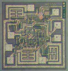
GENERAL DIE INFORMATION
Substrate Thickness (mils) Die size (mils) [mm] Bonding pads Backside metal
Silicon 10±1 (40.157x42.126)
[1.02x1.07] min 3.74 x3.74 mils, 1µm thick, aluminium Backside of the die is coated with 0.5µm GOLD , which makes it compatible with AuSi or AuGe die attach.
All US Microwaves products are available in die form. Typical delivery for die products is 2-3 weeks ARO. For Custom designs, delivery is 3-4 weeks ARO. Certain items may be available from stock. Inventory is periodically updated. All devices for chip and wire applications are 100% tested, visual inspected and shipped in waffle packs (WP). For high volume automated assembly, MIS chip capacitors are supplied as 4" wafers 100% tested, inked and diced on expanded film frame (FF).
TECHNOLOGY DESCRIPTION: SEMICONDUCTOR-MANUFACTURING
These integrated Circuits are manufactured with medium voltage junction isolated bipolar process. junction isolated bipolar processes allow integration of high performance NPN, PNP and JFET transistors, MOS capacitors, diffused resistors and precision thin film resistors. The bond pad metallization is standard 1µm Aluminium. The backside of the die is coated with 0.5µm GOLD , which makes it compatible with AuSi or AuGe die attach.
DIE LAYOUT - MECHANICAL SPECIFICATIONS
PAD # FUNCTION X(mils) X(mm) Y(mils) Y(mm)
1 GND 3.740 0.095 12.401 0.315
2 Trigger 4.527 0.115 4.921 0.125
3 Out 23.228 0.590 4.921 0.125
4 Reset 31.889 0.810 17.716 0.450
5 Control 30.708 0.780 32.677 0.830
6 Threshold 31.889 0.810 25 0.635
7 Discharge 16.535 0.420 35.236 0.895
8 Vcc 4.921 0.125 19.291 0.490
STANDARD PRODUCTS ORDERING INFORMATION
STANDARD PRODUCTS PRICE LIST
USM PART # MINIMUM ORDER QUANTITY Waffle Packs U/P($)
USMLM555 100pc -WP $3.20
List prices are for standard products, available from stock.
List prices for other quantities and tolerances are available on line through Instant Quote.
For standard products available from stock, there is a minimum line item order. For custom products
please inquire by contacting US Microwaves technical sales. No rights can be derived from pricing
information provided on this website. Such information is indicative only, is showed for budgetary
use only and subject to change by US MICROWAVES at any time and without notice.
Products sold for space, military or medical applications, element evaluation and/or level K or S qualification are subject to minimum order levels to be established on a case by case basis. For any special applications, die level KGD qualification requirements, different packaging or custom configurations, contact sales department.
INSTANT QUOTE
US Microwaves P/N Quantity E-mail
ORDERING: Order on line at: http://www.usmicrowaves.com/porder.htm. A copy of the order along with an order confirmation receipt is issued instantly for all orders placed on line. On line Orders have to be verified, accepted and acknowledged by US Microwaves sales department in writing before, becoming non cancelable binding contracts.
DELIVERY: Typical delivery for die products packaged in waffle packs is 2-4 weeks ARO. For Custom designs, delivery is 3-5 weeks ARO. Certain items may be available from stock with delivery up to 1 week.
SHIPPING/PACKAGING: All devices for chip and wire applications are 100% tested, visual inspected and shipped in waffle packs (WP).
SAMPLES: Samples are available only for customers that have issued firm orders pending qualification of product in a particular application.
GUARANTEED SUPPLY! US Microwaves guarantees continuous supply and availability of all standard products provided minimum order quantities are met.
U.S. Microwaves has made every effort to have this information as accurate as possible. However, no responsibility is assumed by U.S. Microwaves for its use, nor for any infringements of rights of third parties which may result from its use. U.S. Microwaves reserves the right to revise the content or modify its product line without prior notice. U.S. Microwaves products are not authorized for and should not be used within support systems which are intended for surgical implants into the body, to support or sustain life, in aircraft, space equipment, submarine, or nuclear facility applications without the specific written consent of U.S. Microwaves.
|