|
DUAL LOW POWER OPERATIONAL AMPLIFIERS
USM LM 358
FEATURES
APPLICATIONS
DUAL LOW POWER OPERATIONAL AMPLIFIERS
Short Circuit Protected Outputs
True Differential Input Stage
Single Supply Operation: 3.0 V to 32 V
Low Input Bias Currents
Internally Compensated
Common Mode Range Extends to Negative Supply
Single and Split Supply Operation; Similar Performance to the Popular MC1558
ESD Clamps on the Inputs Increase Ruggedness of the Device without Affecting Operation
In DIE form, this device is an excellent selection for many chip and wire HYBRID CIRCUITS.
PRODUCT DESCRIPTION AND SHORT APPLICATION NOTE
Utilizing the circuit designs perfected for recently introduced Quad Operational Amplifiers, these dual operational amplifiers feature 1) low power drain, 2) a common mode input voltage range extending to ground/VEE , 3) single supply or split supply operation and 4) pin outs compatible with the popular MC1558 dual operational amplifier. These amplifiers have several distinct advantages over standard operational amplifier types in single supply applications. They can operate at supply voltages as low as 3.0 V or as high as 32 V, with quiescent currents about one-fifth of those associated with the MC1741 (on a per amplifier basis). The common mode input range includes the negative supply, thereby eliminating the necessity for external biasing components in many applications. The output voltage range also includes the negative power supply voltage.
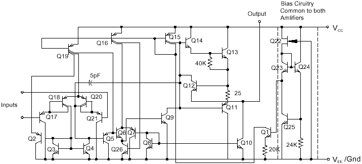
IC SCHEMATIC DIAGRAM
MAXIMUM RATINGS
PARAMETER SYMBOL VALUE UNITS
Power Supply Voltage
Single Supply VCC 32 V
Split Supplies VCC, VEE ±16 V
Input Differential Voltage Range (Note 1) VDIR ±32 V
Input Common Mode Voltage Range (Note 2) VICR -0.3 to 32 V
Output Short Circuit Duration Tsc Continuous
Junction Temperature TJ 150 °C
Storage Temperature Range Tstg -55 to +125 °C
Operating Ambient Temperature Range TA 0 to +70 °C
ONLY Proper die handling equipment and procedures should be employed. Stresses beyond listed absolute maximum ratings may cause permanent damage to the device.
ELECTRICAL CHARACTERISTIC
PARAMETER TEST CONDITIONS SYMBOL MIN TYP MAX UNITS
Input Offset Voltage VCC=5.0V to 30V
VIC=0V to VCC=1.7V
VO=1.4V, RS=0W
TA=25°C
TA=Thigh (Note 1)
TA=Tlow (Note 1) VIO
2.0
7.0
9.0
9.0
mV
Average Temperature
Coefficient of Input Offset Voltage TA=Thigh to Tlow (Note 1)
7.0
µV/°C
Input Offset Current
Input Bias Current
TA=Thigh to Tlow (Note 1)
TA=Thigh to Tlow (Note 1)
IIO 5.0
-
-45
-50 30
75
-250
-500 nA
Average Temperature Coefficient of Input Offset Voltage TA=Thigh to Tlow (Note 1) 10 pA/°C
Input Common Mode Voltage Range (Note 2) VCC=30V
VCC=30V
TA=Thigh to Tlow (Note 1) VICR 0
0 28.3
28 V
Large Signal Open Loop Voltage Gain RL=2.0kOhm, VCC=15V, for Large VOSwing,
TA=Thigh to Tlow (Note 1) AVOL
25
15
100
-
-
-
V/mV
Channel Separation 1.0kHz =< f =< 20kHz Input Referenced CS
- -120 - dB
Common Mode Rejection RS =< 10kW CMR 65 70 dB
Power Supply Rejection PSR 65 100 dB
Output Voltage-High Limit (TA=Thigh to Tlow) (Note 1)
VCC=5.0V, RL=2.0kW,
TA=25°C
VCC=30V, RL=2.0kW
VCC=30V, RL=10kW VOH
3.3
26
27
3.5
-
28
-
-
-
V
Output Voltage-Low Limit VCC=5.0V, RL=10kW
(TA=Thigh to Tlow) (Note 1) VOL
- 5 20 mV
Output Source Current VID=+1.0V, VCC=15V IO + 20 40 mA
Output Sink Current VID=-1.0V, VCC=15V
VID=-1.0V, VCC=200mV IO - 10
12 20
50 -
- mA
µA
Output Short Circuit to Ground (Note 3) ISC - 40 60 mA
Power Supply Current
TA=Thigh to Tlow (Note 1)
VCC=30V, VO=0V, RL=¥
VCC=5.0V, VO=0V, RL=¥ ICC
-
-
1.5
0.7
3.0
1.2 mA
Differential Input Voltage Range VIDR VCC V
(NOTE 1)Tlow=0°C for USM358, Thigh=+70°C for USM358,
(NOTE 2)The input common mode voltage or either input signal voltage should not be allowed to go negative by more than 0.3V. The upper end of the common mode voltage range is VCC -1.7V.
(NOTE 3)Short circuits from the output to VCC can cause excessive heating and eventual destruction. Destructive dissipation can result from simultaneous shorts on all amplifiers.
GENERAL DIE INFORMATION
Substrate Thickness (mils) Die size (mils) [mm] Bonding pads Backside metal
Silicon 10±1 (64.961x35.433)(mils) [1.65x0.9][mm] 4.724x4.724(mils) Backside of the die is coated with 0.5µm GOLD , which makes it compatible with AuSi or AuGe die attach.
All US Microwaves products are available in die form. Typical delivery for die products is 2-3 weeks ARO. For Custom designs, delivery is 3-4 weeks ARO. Certain items may be available from stock. Inventory is periodically updated. All devices for chip and wire applications are 100% tested, visual inspected and shipped in waffle packs (WP). For high volume automated assembly, MIS chip capacitors are supplied as 4" wafers 100% tested, inked and diced on expanded film frame (FF).
TECHNOLOGY DESCRIPTION: SEMICONDUCTOR-MANUFACTURING
These integrated Circuits are manufactured with medium voltage junction isolated bipolar process. junction isolated bipolar processes allow integration of high performance NPN, PNP and JFET transistors, MOS capacitors, diffused resistors and precision thin film resistors. The bond pad metallization is standard 1µm Aluminium. The backside of the die is coated with 0.5µm GOLD , which makes it compatible with AuSi or AuGe die attach.
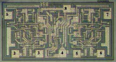
DIE LAYOUT - MECHANICAL SPECIFICATIONS
PAD # FUNCTION X(mils) X(mm) Y(mils) Y(mm)
1 #1 OUT 3.346 0.085 24.606 0.625
2 #1 IN- 7.165 0.182 3.465 0.088
3 #1 IN+ 20.394 0.518 3.465 0.088
4 GND 33.268 0.845 3.465 0.088
5 #2 IN+ 41.142 1.045 3.465 0.088
6 #2 IN- 54.370 1.381 3.465 0.088
7 #2 OUT 58.189 1.478 24.606 0.625
8 VCC 35.787 0.909 28.346 0.720
STANDARD PRODUCTS ORDERING INFORMATION
STANDARD PRODUCTS PRICE LIST
USM PART # MINIMUM ORDER QUANTITY Waffle Packs U/P($)
USMLM358 100pc -WP $3.20
List prices are for standard products, available from stock.
List prices for other quantities and tolerances are available on line through Instant Quote.
For standard products available from stock, there is a minimum line item order. For custom products
please inquire by contacting US Microwaves technical sales. No rights can be derived from pricing
information provided on this website. Such information is indicative only, is showed for budgetary
use only and subject to change by US MICROWAVES at any time and without notice.
Products sold for space, military or medical applications, element evaluation and/or level K or S qualification are subject to minimum order levels to be established on a case by case basis. For any special applications, die level KGD qualification requirements, different packaging or custom configurations, contact sales department.
INSTANT QUOTE
US Microwaves P/N Quantity E-mail
ORDERING: Order on line at: http://www.usmicrowaves.com/porder.htm. A copy of the order along with an order confirmation receipt is issued instantly for all orders placed on line. On line Orders have to be verified, accepted and acknowledged by US Microwaves sales department in writing before, becoming non cancelable binding contracts.
DELIVERY: Typical delivery for die products packaged in waffle packs is 2-4 weeks ARO. For Custom designs, delivery is 3-5 weeks ARO. Certain items may be available from stock with delivery up to 1 week.
SHIPPING/PACKAGING: All devices for chip and wire applications are 100% tested, visual inspected and shipped in waffle packs (WP).
SAMPLES: Samples are available only for customers that have issued firm orders pending qualification of product in a particular application.
GUARANTEED SUPPLY! US Microwaves guarantees continuous supply and availability of all standard products provided minimum order quantities are met.
U.S. Microwaves has made every effort to have this information as accurate as possible. However, no responsibility is assumed by U.S. Microwaves for its use, nor for any infringements of rights of third parties which may result from its use. U.S. Microwaves reserves the right to revise the content or modify its product line without prior notice. U.S. Microwaves products are not authorized for and should not be used within support systems which are intended for surgical implants into the body, to support or sustain life, in aircraft, space equipment, submarine, or nuclear facility applications without the specific written consent of U.S. Microwaves.
|