|
ADJUSTABLE PRECISION SHUNT REGULATOR
USM AS 431
FEATURES
APPLICATIONS
ADJUSTABLE PRECISION SHUNT REGULATOR
Average temperature coefficient 50ppm/° C
Temperature compensated for operation over the full temperature range
Programmable output voltage
Fast turn-on response
Low out put noise
In DIE form, this device is an excellent selection for many chip and wire HYBRID CIRCUITS.
PRODUCT DESCRIPTION AND SHORT APPLICATION NOTE
The USM AS431 is a 3-terminal adjustable shunt regulator with guaranteed temperature stability over the entire temperature range of operation. It is now available in a chip sized package(4-Bump micro SMD )using National’s micro SMD package technology. The output voltage may be set at any level greater than 2.5V (VREF) up to 36V merely by selecting two external resistors that act as a voltage divided network.Due to the sharp turn-on characteristics this device is an excellent replacement for many zener diode applications.
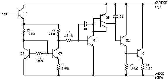
IC SCHEMATIC DIAGRAM
MAXIMUM RATINGS
PARAMETER SYMBOL VALUE USM431 UNITS
Storage Temperature Range 65°C to +150 °C
Operating Temperature Range
Industrial (LM431xl)
Commercial (LM431xC)
40 to +85
0to +70 °C
Infrared or Convection(20sec.)235 C 235 °C
Wave Soldering (10sec.) 260(lead temp.) °C
Cathode Voltage 37 V
ContinuousCathodeCurrent -10 to +150 mA
Reference Voltage - 0.5 V
Reference Input Current 10 mA
ONLY Proper die handling equipment and procedures should be employed. Stresses beyond listed absolute maximum ratings may cause permanent damage to the device.
ELECTRICAL CHARACTERISTIC
TA=25°C unless otherwise specificed
PARAMETER TEST CONDITIONS SYMBOL MIN TYP MAX UNITS
Reference Voltage VZ=VREF,II =10mA LM431A
VZ=VREF,II=10mA LM431B
VZ=VREF,II=10mA LM431C VREF 2.440
2.470
2.485 2.495
2.495
2.500 2.550
2.520
2.510 V
Deviation of Reference Input Voltage Over Temperature (Note5) VZ=VREF,II=10mA TA= Full Range VDEV 8 17 mV
Ratio of the Change in Reference Voltage to the Change in Cathode Voltage IZ=10mA,
(LM431B) VZ from VREF to10V DVREF/DVZ -1.4
-1.0
-2.7
-2.0 mV/V
VZfrom 10V to 36V
Reference Input Current R1=10k W,R2=¥,IL =10mA(LM431B) IREF 2.0 4.0 µA
Deviation of Reference Input Current over Temperature R1=10kW ,R2=¥,IL=10mA,TA= Full Range(LM431B) µIREF 0.4 1.2 µA
Minimum Cathode Current for Regulation VZ=VREF(LM431A) IZ(MIN) 0.4 1.0 µA
Off-State Current VZ=36V,VREF =0V(LM431C) IZ(OFF) 0.3 1.0 µA
Dynamic Output Impedance (Note6) VZ=VREF Frequency=0 Hz (LM431A)
VZ=VREF Frequency=0 Hz (LM431B,LM431C) rZ 0.75
0.50 W
(NOTE 1)Absolute Maximum Ratings indicate limits beyond which damage to the device may occur.Electrical specifications do not apply when operating the device beyond its rated operating conditions.
(NOTE 2)TJMAX=150 °C
(NOTE 3)Ratings apply to ambient temperature at 25 °C.Above this temperature,derate the TO-92 at 6.2mW/ °C,the SO-8 at 6.5mW/°C,the SOT-23 at 2.2mW/ °C and the micro SMD at 3mW/ °C
(NOTE 4)Deviation of reference input voltage,VDEV,is defined as the maximum variation of the reference input voltage over the full temperature range.
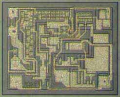
GENERAL DIE INFORMATION
Substrate Thickness (mils) Die size (mils) [mm] Bonding pads Backside metal
Silicon 10±1 (40.5x33.5)[1.03x0.85] min 4x4 mils, 1µm thick, aluminium Backside of the die is coated with 0.5µm GOLD , which makes it compatible with AuSi or AuGe die attach.
All US Microwaves products are available in die form. Typical delivery for die products is 2-3 weeks ARO. For Custom designs, delivery is 3-4 weeks ARO. Certain items may be available from stock. Inventory is periodically updated. All devices for chip and wire applications are 100% tested, visual inspected and shipped in waffle packs (WP). For high volume automated assembly, MIS chip capacitors are supplied as 4" wafers 100% tested, inked and diced on expanded film frame (FF).
TECHNOLOGY DESCRIPTION: SEMICONDUCTOR-MANUFACTURING
These integrated Circuits are manufactured with medium voltage junction isolated bipolar process. junction isolated bipolar processes allow integration of high performance NPN, PNP and JFET transistors, MOS capacitors, diffused resistors and precision thin film resistors. The bond pad metallization is standard 1µm Aluminium. The backside of the die is coated with 0.5µm GOLD , which makes it compatible with AuSi or AuGe die attach.
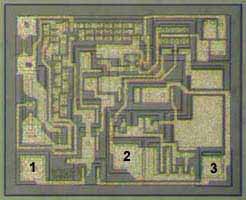
DIE LAYOUT - MECHANICAL SPECIFICATIONS
PAD # FUNCTION X(mils) X(mm) Y(mils) Y(mm)
1 Reference 0.159 6.260 0.158 6.220
2 Anode 0.524 20.630 0.203 7.992
3 Cathode 0.872 34.331 0.158 6.220
STANDARD PRODUCTS PRICE LIST
USM PART # MINIMUM ORDER QUANTITY Waffle Packs U/P($)
USMAS431 100pc -WP $3.20
List prices are for standard products, available from stock.
List prices for other quantities and tolerances are available on line through Instant Quote.
For standard products available from stock, there is a minimum line item order. For custom products
please inquire by contacting US Microwaves technical sales. No rights can be derived from pricing
information provided on this website. Such information is indicative only, is showed for budgetary
use only and subject to change by US MICROWAVES at any time and without notice.
Products sold for space, military or medical applications, element evaluation and/or level K or S qualification are subject to minimum order levels to be established on a case by case basis. For any special applications, die level KGD qualification requirements, different packaging or custom configurations, contact sales department.
INSTANT QUOTE
US Microwaves P/N Quantity E-mail
ORDERING: Order on line at: http://www.usmicrowaves.com/porder.htm. A copy of the order along with an order confirmation receipt is issued instantly for all orders placed on line. On line Orders have to be verified, accepted and acknowledged by US Microwaves sales department in writing before, becoming non cancelable binding contracts.
DELIVERY: Typical delivery for die products packaged in waffle packs is 2-4 weeks ARO. For Custom designs, delivery is 3-5 weeks ARO. Certain items may be available from stock with delivery up to 1 week.
SHIPPING/PACKAGING: All devices for chip and wire applications are 100% tested, visual inspected and shipped in waffle packs (WP).
SAMPLES: Samples are available only for customers that have issued firm orders pending qualification of product in a particular application.
GUARANTEED SUPPLY! US Microwaves guarantees continuous supply and availability of all standard products provided minimum order quantities are met.
U.S. Microwaves has made every effort to have this information as accurate as possible. However, no responsibility is assumed by U.S. Microwaves for its use, nor for any infringements of rights of third parties which may result from its use. U.S. Microwaves reserves the right to revise the content or modify its product line without prior notice. U.S. Microwaves products are not authorized for and should not be used within support systems which are intended for surgical implants into the body, to support or sustain life, in aircraft, space equipment, submarine, or nuclear facility applications without the specific written consent of U.S. Microwaves.
|