FEATURES
APPLICATIONS
TRANSISTOR DICE
| Low current (max. 100 mA). Low voltage (max. 65 V). |
| General purpose switching and amplification. |
| PNP GENERAL PURPOSE TRANSISTOR USMBC557 FEATURES Low current (max. 100 mA). Low voltage (max. 65 V). APPLICATIONS General purpose switching and amplification. PRODUCT DESCRIPTION AND SHORT APPLICATION NOTE USMBC557 is a general purpose PNP transistor offered in die form, and in a TO-92 or SOT54 plastic package. TECHNOLOGY DESCRIPTION: SEMICONDUCTOR-THIN FILM MANUFACTURING All thin film microwave products are manufactured using advanced semiconductors and thin film technologies including ultra-stable and self passivating Tantalum Nitride resistors, gold interconnect metallization and reliable MNOS capacitors to achieve excellent uniformity, performance and reliability. Thin film technology is the preferred solution for all applications that require low noise, long term stability and excellent performance at very high frequencies. US Microwaves employs proprietary thin film technologies for deposition of a wide range of resistive films with sheet resistance films from 1W/sq to 10,000W/sq. All US Microwaves products are available in die form and are ideal for high reliability hybrid and multi chip module applications. MAXIMUM RATINGS VCBO,Collector-base voltage,open emitter -50 V VCEO,collector-emitter voltage,open base -45 V VEBO,emitter-base voltage,open collector -5 V IC,collector current (DC) -100 mA ICM,peak collector current -200 mA IBM,peak base current -200 mA Ptot,total power dissipation,Tamb 25 °C 500 mW Tstg,storage temperature -65 to +150 °C Tj,junction temperature 150 °C Tamb,operating ambient temperature -65 to +150 °C ONLY Proper die handling equipment and procedures should be employed. Stresses beyond listed absolute maximum ratings may cause permanent damage to the device. ELECTRICAL CHARACTERISTICS (25°C unless otherwise specified) PARAMETER VALUE UNITS ICBO,collector cut-off current,IE = 0; VCB = -30 V typ.-1 max.15 nA ICBO,collector cut-off current,IE = 0; VCB = -30 V,Tj = 150 °C max -4 mA IEBO,emitter cut-off current,IC = 0; VEB = -5 V -100 nA hFE,DC current gain,IC = -2 mA; VCE = -5 V; min 125 max 800 - VCEsat,collector-emitter saturation voltage,IC = -10 mA; IB = -0.5 mA typ.-60 max.-300 mV VCEsat,collector-emitter saturation voltage,IC = -100 mA; IB = -5 mA typ.-180 max-650 mV VBEsat,base-emitter saturation voltage,IC = -10 mA; IBB = -0.5 mA; note 1 typ. -750 mV VBEsat,base-emitter saturation voltage,IC = -100 mA; IB = -5 mA; note 1 typ.-930 mV VBE,base-emitter voltage,IC = -2 mA; VCE = -5 V; note 2 min.-600 typ.-650 max.-750 mV VBE,base-emitter voltage,IC = -10 mA; VCE = -5 V; note 2 max.-820 mV Cc,collector capacitance,IE =ie = 0; VCB = -10 V; f = 1 MHz typ.3 pF Ce,emitter capacitance typ.10 pF fT,transition frequency,IC = -10 mA; VCE = -5 V; f = 100 MHz min 100 MHz F, noise figure,IC = -200 mA; VCE = -5 V; RS =2 kW;f = 1 typ.2 max 10 dB Note 1.VBEsat decreases by about -1.7 mV/K with increasing temperature. Note 2.VBE decreases by about -2 mV/K with increasing temperature. GENERAL DIE INFORMATION Substrate Silicon Thickness 6±1(mils) Die size 15 x 18±1 (mils) Bonding pads min 4x4 mils, 3µm thick, 99.99% electroplated gold with a TiW barrier Backside metal Backside of the die is NOT metallized. Standard TiW/Au or custom metallization is available for special orders. All US Microwaves products are available in die form. Typical delivery for die products is 2-3 weeks ARO. For Custom designs, delivery is 3-4 weeks ARO. Certain items may be available from stock. Inventory is periodically updated. All devices for chip and wire applications are 100% tested, visual inspected and shipped in waffle packs (WP). For high volume automated assembly, MIS chip capacitors are supplied as 4" wafers 100% tested, inked and diced on expanded film frame (FF). STANDARD PRODUCTS ORDERING INFORMATION USM BC557 -WP 100pc $ List prices are for standard products, available from stock. List prices for other quantities and tolerances are available on line through Instant Quote. For standard products available from stock, there is a minimum line item order. For custom products please inquire by contacting US Microwaves technical sales. No rights can be derived from pricing information provided on this website. Such information is indicative only, is showed for budgetary use only and subject to change by US MICROWAVES at any time and without notice. Products sold for space, military or medical applications, element evaluation and/or level K or S qualification are subject to minimum order levels to be established on a case by case basis. For any special applications, die level KGD qualification requirements, different packaging or custom configurations, contact sales department. ORDERING: Order on line at: http://www.usmicrowaves.com/porder.htm. A copy of the order along with an order confirmation receipt is issued instantly for all orders placed on line. On line Orders have to be verified, accepted and acknowledged by US Microwaves sales department in writing before, becoming non cancelable binding contracts. DELIVERY: Typical delivery for die products packaged in waffle packs is 2-4 weeks ARO. For Custom designs, delivery is 3-5 weeks ARO. Certain items may be available from stock with delivery up to 1 week. SHIPPING/PACKAGING: All devices for chip and wire applications are 100% tested, visual inspected and shipped in waffle packs (WP). For larger orders,>10k pc, devices can be shipped on film frame. For smaller quantities, it may vary. For high volume automated assembly, devices may be supplied as 4" wafers 100% tested, inked and diced on expanded film frame (FF). SAMPLES: Samples are available only for customers that have issued firm orders pending qualification of product in a particular application. GUARANTEED SUPPLY! US Microwaves guarantees continuous supply and availability of all standard products provided minimum order quantities are met. U.S. Microwaves has made every effort to have this information as accurate as possible. However, no responsibility is assumed by U.S. Microwaves for its use, nor for any infringements of rights of third parties which may result from its use. U.S. Microwaves reserves the right to revise the content or modify its product line without prior notice. U.S. Microwaves products are not authorized for and should not be used within support systems which are intended for surgical implants into the body, to support or sustain life, in aircraft, space equipment, submarine, or nuclear facility applications without the specific written consent of U.S. Microwaves. |
| US MICROWAVES | PNP GENERAL PURPOSE TRANSISTOR | |
| Advanced Microwave Components | USMBC557 | |
|
FEATURES
|
APPLICATIONS
|
TRANSISTOR DICE
|
||
|
|
|
| PRODUCT DESCRIPTION AND SHORT APPLICATION NOTE |
| USMBC557 is a general purpose PNP transistor offered in die form, and in a TO-92 or SOT54 plastic package. |
| TECHNOLOGY DESCRIPTION: SEMICONDUCTOR-THIN FILM MANUFACTURING |
|
All thin film microwave products are manufactured using advanced semiconductors and thin film technologies including ultra-stable and self
passivating Tantalum Nitride resistors, gold interconnect metallization and reliable MNOS capacitors to achieve excellent uniformity,
performance and reliability. Thin film technology is the preferred solution for all applications that require low noise, long term stability
and excellent performance at very high frequencies. US Microwaves employs proprietary thin film technologies for deposition of a wide range
of resistive films with sheet resistance films from 1Ω/sq to 10,000Ω/sq. All US Microwaves products are available in die form and are
ideal for high reliability hybrid and multi chip module applications. All US Microwaves products are manufactured using GOLD CHIP TECHNOLOGY™ a trade mark of Semiconix Corporation. |
| MAXIMUM RATINGS | ||
| PARAMETER | VALUE | UNITS |
| VCBO,Collector-base voltage,open emitter | -50 | V |
| VCEO,collector-emitter voltage,open base | -45 | V |
| VEBO,emitter-base voltage,open collector | -5 | V |
| IC,collector current (DC) | -100 | mA |
| ICM,peak collector current | -200 | mA |
| IBM, peak base current | -200 | mA |
| Ptot,total power dissipation,TAMB≤25°C | 500 | mW |
| TSTG, storage temperature | -65 to +150 | °C |
| TJ, junction temperature | 150 | °C |
| TAMB, operating ambient temperature | -65 to +150 | °C |
| ONLY Proper die handling equipment and procedures should be employed. Stresses beyond listed absolute maximum ratings may cause permanent damage to the device. | ||
| ELECTRICAL CHARACTERISTICS | ||
| PARAMETER | VALUE | UNITS |
| ICBO,collector cut-off current, IE=0; VCB=-30V | typ.-1 max.15 | nA |
| ICBO, collector cut-off current, IE=0; VCB=-30V, Tj=150°C | max -4 | µA |
| IEBO, emitter cut-off current, IC=0; VEB=-5V | -100 | nA |
| hFE, DC current gain, IC=-2 mA; VCE=-5V | min 125 max 800 | - |
| VCEsat, collector-emitter saturation voltage, IC=-10mA; IB=-0.5mA | typ.-60 max.-300 | mV |
| VCEsat, collector-emitter saturation voltage, IC=-100mA; IB=-5mA | typ.-180 max -650 | mV |
| VBEsat, base-emitter saturation voltage, IC=-10 mA; IBB=-0.5mA; note 1 | -750 | mV |
| VBEsat, base-emitter saturation voltage, IC=-100 mA; IB=-5mA; note 1 | -930 | mV |
| VBE, base-emitter voltage, IC=-2mA; VCE=-5V; note 2 | min.-600 typ.-650 max. -750 | mV |
| VBE, base-emitter voltage, IC=-10mA; VCE=-5 V; note 2 | max.-820 | mV |
| CC, collector capacitance, IE=0; VCB=-10V; f=1MHz | 3 | pF |
| CE, emitter capacitance | 10 | pF |
| fT, transition frequency, IC=-10mA; VCE=-5V; f=100MHz | ≥100 | MHz |
| F, noise figure, IC=-200mA; VCE=-5V; RS=2kΩ f=1MHz | typ.2 max 10 | dB |
| Note 1.VBEsat decreases by about -1.7 mV/K with increasing temperature.
Note 2.VBE decreases by about -2 mV/K with increasing temperature. |
||
| GENERAL DIE INFORMATION | ||||
| Substrate | Thickness [mils] | Die Size [mils] | Bonding Pads | Backside metal |
| Silicon | 6±1 | 15 x 18±1 | min 4x4 mils, 3µm thick, 99.99% electroplated gold with a TiW barrier | Backside of the die is NOT metallized. Standard TiW/Au or custom metallization is available for special orders. |
| All US Microwaves products are available in die form. Typical delivery for die products is 2-3 weeks ARO. For Custom designs, delivery is 3-4 weeks ARO. Certain items may be available from stock. Inventory is periodically updated. All devices for chip and wire applications are 100% tested, visual inspected and shipped in waffle packs (WP). For high volume automated assembly, MIS chip capacitors are supplied as 4" wafers 100% tested, inked and diced on expanded film frame (FF). | ||||
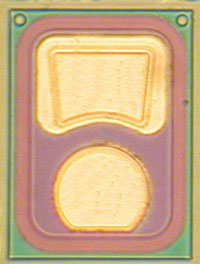
| DIE LAYOUT |
|
| STANDARD PRODUCTS ORDERING INFORMATION |
| STANDARD PRODUCTS PRICE LIST | |||
| USM PART # | Waffle Packs | MINIMUM ORDER QUANTITY | U/P($) |
| USM BC557 | -WP | 100pc | |
| List prices are for standard products, available from stock. List prices for other quantities and tolerances are available on line through Instant Quote. For standard products available from stock, there is a minimum line item order. For custom products please inquire by contacting US Microwaves technical sales. No rights can be derived from pricing information provided on this website. Such information is indicative only, is showed for budgetary use only and subject to change by US MICROWAVES at any time and without notice. | |||
| Products sold for space, military or medical applications, element evaluation and/or level K or S qualification are subject to minimum order levels to be established on a case by case basis. For any special applications, die level KGD qualification requirements, different packaging or custom configurations, contact sales department. | |||
| ORDERING: Order on line at: http://www.usmicrowaves.com/porder.htm. A copy of the order along with an order confirmation receipt is issued instantly for all orders placed on line. On line Orders have to be verified, accepted and acknowledged by US Microwaves sales department in writing before, becoming non cancelable binding contracts.
DELIVERY: Typical delivery for die products packaged in waffle packs is 2-4 weeks ARO. For Custom designs, delivery is 3-5 weeks ARO. Certain items may be available from stock with delivery up to 1 week. SHIPPING/PACKAGING: All devices for chip and wire applications are 100% tested, visual inspected and shipped in waffle packs (WP). For larger orders,>10k pc, devices can be shipped on film frame. For smaller quantities, it may vary. For high volume automated assembly, devices may be supplied as 4" wafers 100% tested, inked and diced on expanded film frame (FF). SAMPLES: Samples are available only for customers that have issued firm orders pending qualification of product in a particular application. |
| GUARANTEED SUPPLY! US Microwaves guarantees continuous supply and availability of all standard products provided minimum order quantities are met. |
| U.S. Microwaves has made every effort to have this information as accurate as possible. However, no responsibility is assumed by U.S. Microwaves for its use, nor for any infringements of rights of third parties which may result from its use. U.S. Microwaves reserves the right to revise the content or modify its product line without prior notice. U.S. Microwaves products are not authorized for and should not be used within support systems which are intended for surgical implants into the body, to support or sustain life, in aircraft, space equipment, submarine, or nuclear facility applications without the specific written consent of U.S. Microwaves. |
| Home | Product Tree | Tech. Support | Print PDF | Request Quote | Inventory | Place Order | Contact sales |
| Last updated: November 14, 2012 | |
| US MICROWAVES | Tel:408-758-8690 Fax: 408-986-8027 | USMICROWAVES |
| ©1990-2026 US MICROWAVES All rights reserved. No material from this site may be used or reproduced without permission. |