LM7805A die equivalent, USM LM7805A die  is a 3-terminal positive voltage regulator designed with built in  internal current limiting, thermal shutdown and safe-area compensation for maximum flexibility and safety . With adequate heat sinking provided, USM LM7805A can deliver up to 1.5A output current. USM LM7805A can be used as fixed voltage regulator in a wide range of applications where local voltage regulation is preferred for elimination of noise and distribution problems associated with single-point regulation. USM LM7805A can also be used (by adding external components) to obtain adjustable output voltages and currents. It is not necessary to bypass the output, although this does improve transient response. Input bypassing is needed only if the regulator is located far from the filter capacitor of the power supply. USM LM7805A is available in die form only. Die size is 80x80mils. Die thickness is 10 mils  +/- 1mils. The bond pad metallization is standard 1µm Aluminum. Backside of the die is coated with 0.5µm GOLD , which makes it compatible with AuSi or AuGe die attach.


US MICROWAVES
Advanced Microwave Components
  5V POSITIVE VOLTAGE REGULATOR DIE FOR HYBRID CIRCUITS
USM LM7805A
PART HAS BEEN REPLACED BY USM LM7805H


FEATURES
APPLICATIONS
VOLTAGE REGULATOR
Output Current in Excess of 1A
Output Voltages of +5V
Internal Thermal Overload Protection
Short Circuit Protection
Output Transistor Safe
Operating area Compensation
In DIE form, this device is an excellent selection for many chip and wire HYBRID CIRCUITS

PRODUCT DESCRIPTION AND SHORT APPLICATION NOTE
USM LM7805A is a 3-terminal positive voltage regulator designed with built in internal current limiting, thermal shutdown and safe-area compensation for maximum flexibility and safety . With adequate heat sinking provided, USM LM7805A can deliver up to 1.5A output current. USM LM7805A can be used as fixed voltage regulator in a wide range of applications where local voltage regulation is preferred for elimination of noise and distribution problems associated with single-point regulation. USM LM7805A can also be used (by adding external components) to obtain adjustable output voltages and currents.
It is not necessary to bypass the output, although this does improve transient response. Input bypassing is needed only if the regulator is located far from the filter capacitor of the power supply.
USM LM7805A is available in die form only. The die size is 66.93x72.83mils. The die thickness is 16.5±1 mils. The bond pad metallization is standard 1µm Aluminum. The backside of the die is coated with 0.5µm GOLD , which makes it compatible with AuSi or AuGe die attach.


IC SCHEMATIC DIAGRAM

MAXIMUM RATINGS
PARAMETER SYMBOL VALUE UNITS
Internal Power Dissipation (Note1) PD internally limited W
Input Voltage VIN 35 V
Maximum Junction Temperature TJ 150 °C
Operating Junction Temperature Range TJ 0 to 150 °C
Storage Temperature Range TSTG -65 to +150 °C
ESD Susceptibility   2  
ONLY Proper die handling equipment and procedures should be employed. Stresses beyond listed absolute maximum ratings may cause permanent damage to the device.

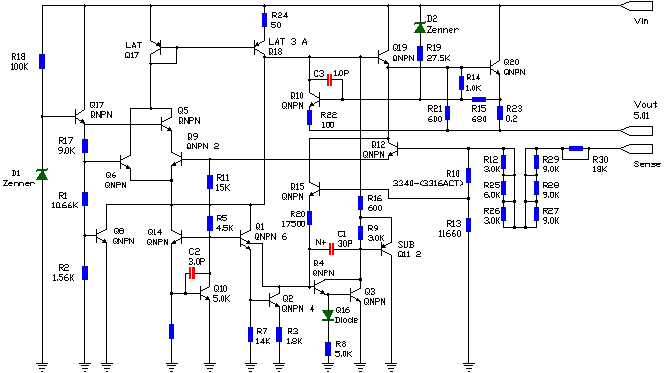
ELECTRICAL CHARACTERISTIC
–55°C<Tj<+150°C, Vi = 10V, Io = 500mA, Ci = 0.33µF, Co= 0.1µF, unless otherwise specified
PARAMETER TEST CONDITIONS SYMBOL MIN TYP MAX UNITS
Output Voltage Tj=25 ° C VO 4.8 5.0 5.2 V
Line Regulation
Tj = 25 °C 7.0V<Vi<25V
                      8.0V<Vi<12V
DVO     100
50
mV
Load Regulation Tj = 25 °C 5.0mA < IO < 1.5A
                       250mA < IO< 750mA
DVO     100
50
mV
Output Voltage
7.0V<Vi<20V, 5.0mA<Io<1.0A, 0°C<Tj <125°C
Vo 4.75   5.25 V
Quiescent Current Tj = 25 °C Iq      8 mA
Quiescent Current With Line With Load
7V < Vi < 25V
5.0mA < Io < 1.0A
DIq     1.3
0.5
mA
Noise Ta=25°C, 10Hz < f < 100kHz Vn     40 µV
Ripple Rejection
f=120Hz, Io=350mA, Tj=25°C
DV1/DVo 62 80   dB
Dropout Voltage Io=1.0A, Tj=25°C Vdo   2.0   V
Output Resistance
f=1.0kHz
Ro   8   mW
Output Short Circuit Current Tj = 25°C, Vj = 35V Ios     2.1 A
Average Temperature Coefficient of Output Voltage
–55°C < Ta < +250°C, Io < 5mA
DVo/DT   0.6 -4.0 mV/°C
 
(NOTE 1)Load and line regulation are specified at constant junction temperature. Changes in Vo due to heating effects have to be added to those due to the Io. The device should be subject to low duty cycle pulses ONLY.
(NOTE 2)All characteristics are measured with a 0.22µF capacitor from input to ground and a 0.1µF capacitor from output to ground. All characteristics except noise voltage and ripple rejection ratio are measured using pulse techniques (tw<10ms, duty cycle<5%). Output voltage changes due to changes in internal temperature must be taken into account separately.

GENERAL DIE INFORMATION
Substrate Thickness (mils) Die size (mils) [mm] Bonding pads Backside metal
Silicon 16±1 (66.93x72.83)[1.70x1.85] min 9.5x9.5 mils Backside of the die is coated with 0.5µm GOLD , which makes it compatible with AuSi or AuGe die attach.
All US Microwaves products are available in die form. Typical delivery for die products is 2-3 weeks ARO. For Custom designs, delivery is 3-4 weeks ARO. Certain items may be available from stock. Inventory is periodically updated. All devices for chip and wire applications are 100% tested, visual inspected and shipped in waffle packs (WP). For high volume automated assembly, MIS chip capacitors are supplied as 4" wafers 100% tested, inked and diced on expanded film frame (FF).

TECHNOLOGY DESCRIPTION: SEMICONDUCTOR-MANUFACTURING
These integrated Circuits are manufactured with medium voltage junction isolated bipolar process. junction isolated bipolar processes allow integration of high performance NPN, PNP and JFET transistors, MOS capacitors, diffused resistors and precision thin film resistors. The bond pad metallization is standard 1µm Aluminium. The backside of the die is coated with 0.5µm GOLD , which makes it compatible with AuSi or AuGe die attach.
All US Microwaves products are manufactured using GOLDCHIP TECHNOLOGY™ a trade mark of Semiconix Corporation.

DIE LAYOUT - MECHANICAL SPECIFICATIONS
PAD # FUNCTION X(mm) Y(mm) Bond Pad (mm)
1 Input 710 775 270x365
2 GND -750 -825 265x240
3 Output -750 -825 300x400
Note: Origin is the center of the die.


STANDARD PRODUCTS ORDERING INFORMATION

STANDARD PRODUCTS PRICE LIST
USM PART # MINIMUM ORDER QUANTITY Waffle Packs U/P($)
USM LM7805A $320/100pc. -WP $3.20
List prices are for standard products, available from stock. List prices for other quantities and tolerances are available on line through Instant Quote. For standard products available from stock, there is a minimum line item order. For custom products please inquire by contacting US Microwaves technical sales. No rights can be derived from pricing information provided on this website. Such information is indicative only, is showed for budgetary use only and subject to change by US MICROWAVES at any time and without notice.
Products sold for space, military or medical applications, element evaluation and/or level K or S qualification are subject to minimum order levels to be established on a case by case basis. For any special applications, die level KGD qualification requirements, different packaging or custom configurations, contact sales department.

INSTANT QUOTE
US Microwaves P/N Quantity E-mail    
 

ORDERING: Order on line at: http://www.usmicrowaves.com/porder.htm. A copy of the order along with an order confirmation receipt is issued instantly for all orders placed on line. On line Orders have to be verified, accepted and acknowledged by US Microwaves sales department in writing before, becoming non cancelable binding contracts.
DELIVERY: Typical delivery for die products packaged in waffle packs is 2-4 weeks ARO. For Custom designs, delivery is 3-5 weeks ARO. Certain items may be available from stock with delivery up to 1 week.
SHIPPING/PACKAGING: All devices for chip and wire applications are 100% tested, visual inspected and shipped in waffle packs (WP).
SAMPLES: Samples are available only for customers that have issued firm orders pending qualification of product in a particular application.

GUARANTEED SUPPLY! US Microwaves guarantees continuous supply and availability of all standard products provided minimum order quantities are met.

U.S. Microwaves has made every effort to have this information as accurate as possible. However, no responsibility is assumed by U.S. Microwaves for its use, nor for any infringements of rights of third parties which may result from its use. U.S. Microwaves reserves the right to revise the content or modify its product line without prior notice. U.S. Microwaves products are not authorized for and should not be used within support systems which are intended for surgical implants into the body, to support or sustain life, in aircraft, space equipment, submarine, or nuclear facility applications without the specific written consent of U.S. Microwaves.

Home Product Tree Tech. Support Print PDF Request Quote Inventory Place Order Contact sales

Last updated: June 21, 2023
US MICROWAVES | Tel:408-758-8690 Fax: 408-986-8027 | USMICROWAVES

©1990-2024 US MICROWAVES All rights reserved. No material from this site may be used or reproduced without permission.