|
US Microwave Quartz Chip Capacitors Lab Kits. US Microwaves recognizes the importance of Lab Kits of Quartz Capacitors for it's Customers. Since the range of capacitance is wide, we found that it is more practical for our customers to choose their own devices in a kit. The following constrains do apply: 1)-maximum number of different capacitance values in a kit is 4 (four). 2)-Maximum quantity in a kit is 100 pc. 3)-The U/P for each kit (100pc/kit) of up to 4 values is $320.00. There is no need for request for quote. Customers can place orders direct from this site or by Fax:(408)986-8027. For other inquiries please contact factory via CONTACTS PAGE or by telephone at 408-986-8026.
SINGLE LAYER QUARTZ
DIELECTRIC CHIP CAPACITORS FEATURES Very high Q over wide range of frequencies 2GHz to 40 GHz. Low
insertion loss <0.08dB from 2GHz to 18GHz High reliability and ruggedness characteristic of semiconductor devices Low temperature
coefficient and wide operating temperature range. Single layer quartz chip capacitors lab
kits are available from stock: Lab-Kit Custom designs are available upon request. Applications Applications of quartz
chip capacitors in microwave hybrid circuits include DC blocks, capacitive coupling, RF bypass capacitors, capacitive loads,
fixed tuning of oscillators, multipliers, tuning of filters and matching networks, switch and comb generators, FET chip mounting.
PRODUCT DESCRIPTION AND SHORT APPLICATION NOTE USMCQXXXX Series is designed to facilitate bread-boarding or to use where a
trimming capability is required. By connecting the pads in parallel the capacitance values are additive, so many combinations
are possible. The CQ Series of single layer quartz chip capacitors are designed to be used as RF bypass, DC blocks, coupling
filter elements and microwave circuit resonant elements. When used as resonant elements in oscillators, Q has to be as high
as possible while the temperature coefficient has to be as small as possible. U.S. Microwaves’ advanced semiconductor and
thin film technologies allow for an important reduction of the series resistance DCR which is increasing the SRF of the capacitor.
High quality dielectrics with low loss factors translates into an increased Q. These devices can be used over the full military
temperature range -55°C to +125°C. Quality and workmanship is per MIL-S-883. Devices are 100% tested, visual inspected and
packaged in waffle packs. The CQ series of chip capacitors are manufactured on quartz and designed to satisfy the requirements
of prototype development and circuit trimming in hybrid packages through selective wire-bonding. TECHNOLOGY DESCRIPTION: SEMICONDUCTOR-THIN
FILM MANUFACTURING All thin film microwave products are manufactured using advanced semiconductors and thin film technologies
including ultra-stable and self passivating Tantalum Nitride resistors, gold interconnect metallization and reliable MNOS
capacitors to achieve excellent uniformity, performance and reliability. Thin film technology is the preferred solution for
all applications that require low noise, long term stability and excellent performance at very high frequencies. US Microwaves
employs proprietary thin film technologies for deposition of a wide range of resistive films with sheet resistance films from
1W/sq to 10,000W/sq. All US Microwaves products are available in die form and are ideal for high reliability hybrid and multi
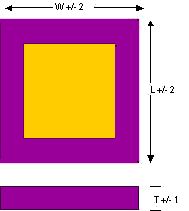
chip module applications. ELECTRICAL CHARACTERISTICS PARAMETER Capacitance range xxx to yyy pF Capacitance Tolerance: Absolute,
+25°C ±20 % DC Resistance typ 0.1 W Breakdown voltage (Bv) 100 V Operating Temperature Range -55
to 125 °C Storage Temperature Range -55 to 125 °C GENERAL DIE INFORMATION Substrate SiO2 / Quartz Thickness (mils) 10±1
19.5±1 Die size (mils) xx x yy ±2 Bonding pads min 4x4 mils, 3µm thick, 99.99% electroplated gold with a TiW barrier Backside
metal Backside of the die is metallized with standard Ti/Pt/Au compatible with Au-Sn, Au-Ge or silver filled conductive epoxy.
Custom metallization is available for special orders. All US Microwaves products are available in die form. Typical delivery
for die products is 2-3 weeks ARO. For Custom designs, delivery is 3-4 weeks ARO. Certain items may be available from stock.
Inventory is periodically updated. All devices for chip and wire applications are 100% tested, visual inspected and shipped
in waffle packs (WP). For high volume automated assembly, MIS chip capacitors are supplied as 4" wafers 100% tested, inked
and diced on expanded film frame (FF). US MICROWAVES manunufacturer of high reliability microwave integrated circuits MIC
technology. US Microwave offers a multitude of applied thin film products and microwave semiconductor devices: manufactures
and supplies high quality standard microwave thin film circuits and microwave devices using advanced technical ceramics and
semiconductor materials; Products include RF micro devices for hybrid chip and wire applications; microwave thin film circuits,
custom manufacturing from customer's data, Quartz Chip Capacitors - ceramic, sapphire and quartz substrate, thin film resistors
- ceramic, silicon and quartz substrates, multi-tap thin film resistors - ceramic and silicon substrates, capacitors MIS for
chip and wire applications, MNOS capacitors, MOS capacitors, ceramic capacitors, Schottky diodes, PIN diodes, tunnel diodes,
SRD diodes, varactor diodes and zero bias diodes, RF NPN and PNP transistors, high speed LDMOS and T MOSFET s, MMIC - RF IC
s silicon and SiGe. SEMICONIX Designs and manufactures standard and custom bipolar and MOS analog devices, semiconductors,
analog integrated circuits, discrete components for high performance systems such as cellular/wireless, video amplifiers,
heart pacemakers and medical imaging systems. Standard semiconductor components are designed and manufactured for space, medical,
telecommunications and military applications only. Company's technology road map is including SiGe epi devices for high speed
RF bipolars and high speed fiber optic and optoelectronic applications. Analog devices, ASIC analog design and manufacturing:
Semiconix produces a series of semi-custom bipolar analog devices in arrays that are customized by designing a specific metal
interconnection mask. The arrays contain a large number of undedicated active and passive components, i.e. transistors, diodes,
resistors, capacitors, MOSFET s, LDMOS, photodiodes, phototransistors, etc. Since wafers are stocked before the metal mask,
the custom IC development phase is shorter and far less expensive compared to conventional full custom ICs. Customers may
provide own analog design. Optoelectronic components: photodiodes, photodiodes arrays, phototransistors, position sensing
devices, optocouplers, optoisolators, photodarlington, high voltage phototransistors output, Schottky infrared detectors.
Discrete semiconductors: Schottky diodes, Zenner diodes, TVS, small signal bipolar transistors, high voltage bipolar transistors,
matched pair bipolar transistors, small signal JFET s and MOSFETs, MCT (MOS controlled tyristors), IGBT. Semiconix 's Divisions:HTE
Labs Provides Wafer Foundry, R&D support and Specialty Wafer Fab Processing to customers from semiconductors and microelectronics
industry. Wafer foundry includes the following processes: 20V, 45V, 75V, 25V super-beta and high voltage dielectric isolated
bipolar process. R&D support is provided in the following fields of microelectronics: thin film active and passive components
technologies, flip chip technology (TiW/Cu/Cu/SnPb), sensor technologies (inertial, pressure, temperature, gas and smoke detectors),
optoelectronic technologies and components, discrete and integrated circuits technology development for special applications,
LiNbO3 applications like SAW, Ti diffused, light wave guides and Mach-Zender light modulators. Specialty wafer fab processing:
epitaxy, SiGe, epi, diffusion and oxidation, ion implant, LPCVD and PECVD Si3N4, SiO2, platinum silicidation, photo-lithography,
plasma etching, silicon micro-machining by KOH anisotropic etch, sputter depositions of Ti/Ni/Ag lift off process, Ti/Pt/Au
lift off process, sputter depositions of thin film resistors: SiCr, NiCr, TaN2, silicon wafers back grind and polish followed
by trimetal backside sputter depositions, gold backside sputter depositions and alloy : gold electroplating and gold bump.
SEMICONWELL designs and manufacture standard and custom Integrated Passive Networks - IPN for the personal computer, telecommunications,
industrial controls, automotive, avionics. The Integrated Passive Networks are a sum of resistors, capacitors, inductors,
diodes and schottky diodes and are available in through hole and surface mounted packages. SEMICONWELL is suppling integrated
termination, filters and ESD protection for use in mobile phones, PDAs, personal computers, notebooks, routers, hubs, internet
appliances. Standard Devices - Most standard devices include resistors, capacitors, inductors, diodes and schottky diodes
networks and are inventoried by the designated part numbers and can be ordered on line, from factory or from distributors.
Custom Devices - Custom IPN (Integrated Passive Networks) are manufactured from customer's prints upon request. US MICROWAVES
develops, manufactures and supplies high quality standard microwave thin film circuits and microwave devices including RF
bipolars for hybrid chip and wire applications as follows: microwave thin film circuits, custom manufacturing from customer's
data, Quartz Chip Capacitors - ceramic, sapphire and quartz substrate, thin film resistors - ceramic, silicon and quartz substrates,
multi-tap thin film resistors - ceramic and silicon substrates, capacitors MIS for chip and wire applications, MNOS capacitors,
MOS capacitors, ceramic capacitors, Schottky,PIN, tunnel, SRD, varactor and zero bias diodes, RF NPN and PNP transistors,
high speed LDMOS and T MOSFET s, MMIC - RF IC s silicon and SiGe. |