|
Spiral chip inductor with high Q and high self resonant frequency: HIGH Q FACTOR CHIP SCALE SPIRAL INDUCTORS GOLD STUD BUMP, 14nH inductance, 5 turns, quartz chip and wire, inductors manufactured by USM LX2500Q20CSP-L05-14nH, spiral chip inductors, low inductance microwave spiral chip inductor with high Q and high self resonant frequency, modeling of spiral chip inductance on quartz substarte for low stray capacitance
keywords: flip chip, flipchip, flip-chip, chip scale, chipscale, chip-scale,low parasitic inductance,chip and wire,wire bonds,thermo compression,conductive epoxy,flip chip mountinginductance,microwave inductors,SPIRAL CHIP INDUCTORS,inductor,RF choke,power supplies,microwave circuit,resonant,thin film,high Q,quartz,Au,TiW,layer,frequency
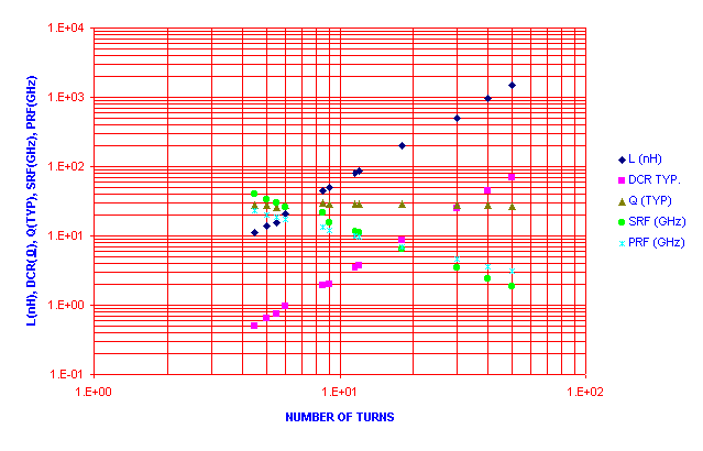
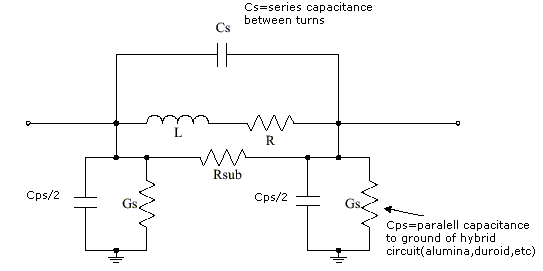
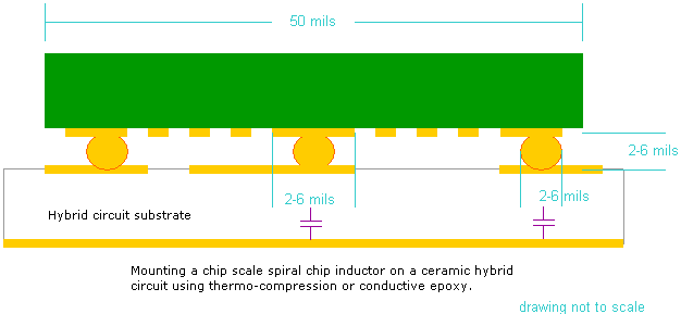
Spiral chip inductor with high Q and high self resonant frequency: HIGH Q FACTOR CHIP SCALE SPIRAL INDUCTORS GOLD STUD BUMP, 14nH inductance, 5 turns, quartz chip and wire, inductors manufactured by USM LX2500Q20CSP-L05-14nH Spiral chip inductor with high Q and high self resonant frequency: HIGH Q FACTOR CHIP SCALE SPIRAL INDUCTORS GOLD STUD BUMP, 14nH inductance, 5 turns, quartz chip and wire, inductors manufactured by USM LX2500Q20CSP-L05-14nH, spiral chip inductors, low inductance microwave spiral chip inductor with high Q and high self resonant frequency, modeling of spiral chip inductance on quartz substarte for low stray capacitance keywords: flip chip, flipchip, flip-chip, chip scale, chipscale, chip-scale,low parasitic inductance,chip and wire,wire bonds,thermo compression,conductive epoxy,flip chip mountinginductance,microwave inductors,SPIRAL CHIP INDUCTORS,inductor,RF choke,power supplies,microwave circuit,resonant,thin film,high Q,quartz,Au,TiW,layer,frequency US MICROWAVESAdvanced Microwave Components HIGH Q FACTOR CHIP SCALE SPIRAL INDUCTORS GOLD STUD BUMP LX2500Q20CSP-L05-14nH FEATURES APPLICATIONS SPIRAL CHIP INDUCTOR Spiral chip inductors are available in 3 different die dimensions: - For 1 turn to 21 turns series the die size is 0.050"x0.050"x0.020". - For 1 turn to 12 turns the die size is 0.030"x0.030"x0.020". - For 1 turn to 8 turns the die size is 0.025"x0.025"x0.020". Chip Scale spiral chip inductors have no parasitic inductance because there are no additional wire bonds. -Simple mounting by thermo compression or with conductive epoxy. -Transparent substrate allows flip chip mounting without specialized equipment. -Compatible with various substrates. Spiral chip inductors are manufactured on quartz (SiO2), 20 mils thick, for lowest capacitance and highest SRF and PRF. The LX2500Q20CSP-L05-14nH spiral chip inductors are manufactured on quartz (SiO2), 20 mils thick. These devices can be used over the full military temperature range -55°C to +125°C. Quality and workmanship is per MIL-S-883. Devices are 100% tested, visual inspected and packaged in waffle packs.Spiral Chip Inductors Lab kits are available from stock: L-Kit PRODUCT DESCRIPTION AND SHORT APPLICATION NOTE Flip chip series of spiral chip inductors are designed to be used in chip and wire hybrid circuits as RF choke in biasing circuits, microwave circuit resonant elements and power supplies. When used as chokes, a modest Q is desirable while in oscillators Q has to be as high as possible. US Microwaves advanced thin film technologies allow for an important reduction of the DCR max, which translates into an increased Q. For spirals with w+s=25µm, Q values between 25 and 30 are obtained which represent a better compromise between the two applications. For lowest capacitance and higher self-resonance, the spiral chip inductors are manufactured on 20 mil thick quartz (SiO2) substrates. Chip scale, flip chip spiral inductors eliminate up to 3nH of parasitic inductance associated with the gold wires used for the standard series LX2500Q20CSP-L05-14nH. Eliminating the parasitic inductance improves inductor performance, self-resonance, precision and operability in the high gigahertz range applications. Flip chip spiral chip inductors are easily mounted by thermo compression or conductive epoxy. The ability to be attached with conductive epoxy opens the possibility of using these high Q and ultra high self-resonance inductors on other substrates than gold-coated thin film on ceramic circuits. The fact that the substrate is transparent fused silica is a bonus feature that helps in flip chip mounting operation without sophisticated and expensive equipment. Application notes AN 102, AN 112 and AN 113 are describing assembly methods for best performance. Manufactured with 99.9% pure gold, the spiral inductor chip does not need any protection and can operate even in hostile environments. Designed and manufactured by US Microwaves in 1990 for military and industrial applications, the spiral chip inductors now can find their place in optoelectronic and wireless consumer products as well. TECHNOLOGY DESCRIPTION: SEMICONDUCTOR-THIN FILM MANUFACTURING All thin film microwave products are manufactured using advanced semiconductors and thin film technologies including ultra-stable and self passivating Tantalum Nitride resistors, gold interconnect metallization and reliable MNOS capacitors to achieve excellent uniformity, performance and reliability. Thin film technology is the preferred solution for all applications that require low noise, long term stability and excellent performance at very high frequencies. US Microwaves employs proprietary thin film technologies for deposition of a wide range of resistive films with sheet resistance films from 1W/sq to 10,000W/sq. All US Microwaves products are available in die form and are ideal for high reliability hybrid and multi chip module applications. All US Microwaves products are manufactured using GOLDCHIP TECHNOLOGY™ a trade mark of Semiconix Corporation. ELECTRICAL CHARACTERISTICS PARAMETERVALUEUNITS Number of turns 5 Inductance 14nH Inductance Tolerance: Absolute, +25°C±20.0 % DC Resistancetyp. 1.7 W Current Rating: Max. @ + 70°C typ. 100 mA Quality Factor Q @ 100MHztyp. 27.9 Series Self Resonance SRFtyp. 33GHz Parallell Self Resonance PRFtyp. 19.7GHz Operating Temperature Range- 55 to + 125°C Storage Temperature Range-55 to +125°C GENERAL DIE INFORMATION SubstrateThickness (mils)Die size (mils)Bonding padsBackside metal SiO2 - Quartz20±125x25±3min 4x4 mils, 3µm thick, 99.99% electroplated gold with a TiW barrier Backside of the die is NOT metallized. Standard TiW/Au or custom metallization is available for special orders. All US Microwaves products are available in die form. Typical delivery for die products is 2-3 weeks ARO. For Custom designs, delivery is 3-4 weeks ARO. Certain items may be available from stock. Inventory is periodically updated. All devices for chip and wire applications are 100% tested, visual inspected and shipped in waffle packs (WP). For high volume automated assembly, MIS chip capacitors are supplied as 4" wafers 100% tested, inked and diced on expanded film frame (FF). DIE LAYOUT - MECHANICAL SPECIFICATIONS STANDARD PRODUCTS ORDERING INFORMATION STANDARD PRODUCTS PRICE LIST USM PART #Waffle PacksMINIMUM ORDER QUANTITYU/P($) USM LX2500Q20CSP-L05-14nH-WP100pc$4.80 Products sold for space, military or medical applications, element evaluation and/or level K or S qualification are subject to minimum order levels to be established on a case by case basis. For any special applications, die level KGD qualification requirements, different packaging or custom configurations, contact sales department. INSTANT QUOTE US Microwaves P/NQuantityE-mail ORDERING: Order on line at: http://www.usmicrowaves.com/porder.htm. A copy of the order along with an order confirmation receipt is issued instantly for all orders placed on line. On line Orders have to be verified, accepted and acknowledged by US Microwaves sales department in writing before, becoming non cancelable binding contracts.DELIVERY: Typical delivery for die products packaged in waffle packs is 2-4 weeks ARO. For Custom designs, delivery is 3-5 weeks ARO. Certain items may be available from stock with delivery up to 1 week.SHIPPING/PACKAGING: All devices for chip and wire applications are 100% tested, visual inspected and shipped in waffle packs (WP). For larger orders,>10k pc, devices can be shipped on film frame. For smaller quantities, it may vary. For high volume automated assembly, devices may be supplied as 4" wafers 100% tested, inked and diced on expanded film frame (FF).SAMPLES: Samples are available only for customers that have issued firm orders pending qualification of product in a particular application. GUARANTEED SUPPLY! US Microwaves guarantees continuous supply and availability of all standard products provided minimum order quantities are met. U.S. Microwaves has made every effort to have this information as accurate as possible. However, no responsibility is assumed by U.S. Microwaves for its use, nor for any infringements of rights of third parties which may result from its use. U.S. Microwaves reserves the right to revise the content or modify its product line without prior notice. U.S. Microwaves products are not authorized for and should not be used within support systems which are intended for surgical implants into the body, to support or sustain life, in aircraft, space equipment, submarine, or nuclear facility applications without the specific written consent of U.S. Microwaves. HomeProduct TreeTech. SupportPrint PDFRequest QuoteInventoryPlace OrderContact sales Last updated: US MICROWAVES www.semiconix-semiconductor.com Tel:(408)986-8026 Fax:(408)986-8027 ©1990- US MICROWAVES All rights reserved. No material from this site may be used or reproduced without permission. |


